
Datasheet


Section 19 Power-Down Modes
Rev.7.00 Feb. 14, 2007 page 815 of 1108
REJ09B0089-0700
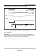
Oscillator
RES
STBY
Oscillation
stabilization
time
Reset
exception
handling
Figure 19.3 Hardware Standby Mode Timing
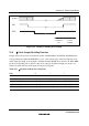
19.8 φ Clock Output Disabling Function
Output of the φ clock can be controlled by means of the PSTOP bit in SCKCR, and DDR for the
corresponding port. When the PSTOP bit is set to 1, the φ clock stops at the end of the bus cycle,
and φ output goes high. φ clock output is enabled when the PSTOP bit is cleared to 0. When DDR
for the corresponding port is cleared to 0, φ clock output is disabled and input port mode is set.
Table 19.5 shows the state of the φ pin in each processing state.
Table 19.5 φ Pin State in Each Processing State
DDR 0 1 1
PSTOP — 0 1
Hardware standby mode High impedance High impedance High impedance
Software standby mode High impedance Fixed high Fixed high
Sleep mode High impedance φ output Fixed high
Normal operating state High impedance φ output Fixed high