
Datasheet


Section 17 ROM
Rev.7.00 Feb. 14, 2007 page 740 of 1108
REJ09B0089-0700
(1) When an interrupt, such as NMI, has occurred during programming/erasing
(2) When the relevant block area of flash memory is read during programming/erasing (including
a vector read or an instruction fetch)
(3) When a SLEEP instruction (including software standby mode) is executed during
programming/erasing
(4) When a bus master other than the CPU, such as DTC or BREQ, has obtained the bus right
during programming/erasing
Error protection is cancelled only by a power-on reset or by hardware-standby mode. Note that the
reset should only be released after providing a reset input over a period longer than the normal 100
μs period. Since high voltages are applied during programming/erasing of the flash memory, some
voltage may remain after the error-protection state has been entered. For this reason, it is
necessary to reduce the risk of damage to the flash memory by extending the reset period so that
the charge is released.
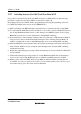
The state-transition diagram in figure 17.75 shows transitions to and from the error-protection
state.
Reset or standby
(Hardware protection)
Program mode
Erase mode
Error protection mode
Error-protection mode
(Software standby)
Read disabled
Programming/erasing
enabled
FLER=0
Read disabled
Programming/erasing disabled
FLER=0
Read enabled
Programming/erasing disabled
FLER=1
Read disabled
programming/erasing disabled
FLER=1
RES = 0 or HSTBY = 0
Error occurrence
Error occurrence
(Software standby)
RES=0 or
HSTBY=0
Software-standby mode
Cancel
software-standby mode
RES=0 or
HSTBY=0
Program/erase interface
register is in its initial state.
Program/erase interface
register is in its initial state.
Figure 17.75 Transitions to and from the Error-Protection State