
Datasheet


Section 17 ROM
Rev.7.00 Feb. 14, 2007 page 717 of 1108
REJ09B0089-0700
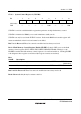
17.23.3 System Control Register 2 (SYSCR2)
Bit : 7 6 5 4 3 2 1 0
— — — — FLSHE — — —
Initial value : 0 0 0 0 0 0 0 0
R/W : — — — — R/W — — R/W
SYSCR2 is an 8-bit readable/writable register that performs on-chip flash memory control.
SYSCR2 is initialized to H'00 by a reset and in hardware standby mode.
SYSCR2 can only be used in the F-ZTAT versions. In the mask ROM versions this register will
return an undefined value if read, and cannot be modified.
Bits 7 to 4—Reserved: These bits cannot be modified and are always read as 0.
Bit 3—Flash Memory Control Register Enable (FLSHE): Controls CPU access to the flash
memory control registers (FCCS, FPCS, FECS, FKEY, FMATS, FTDAR). Writing 1 to the
FLSHE bit enables the flash memory control registers to be read and written to. Clearing FLSHE
to 0 designates these registers as unselected (the register contents are retained).
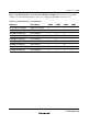
Bit 3
FLSHE
Description
0 Flash control registers are not selected for addresses H'FFFFC4 to H'FFFFCF
(Initial value)
1 Flash control registers are selected for addresses H'FFFFC4 to H'FFFFCF
Bits 2 and 1—Reserved: These bits cannot be modified and are always read as 0.
Bit 0—Reserved: Only 0 may be written to this bit.