
Datasheet


Section 17 ROM
Rev.7.00 Feb. 14, 2007 page 695 of 1108
REJ09B0089-0700
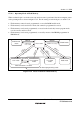
Since the downloaded on-chip program is left in the on-chip RAM after the processing,
download and initialization are not required when the same processing is executed
consecutively.
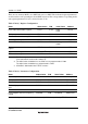
17.22.8 Pin Configuration
Flash memory is controlled by the pin as shown in table 17.47.
Table 17.47 Pin Configuration
Pin Name Abbreviation Input/Output Function
Reset RES Input Reset
Mode 2 MD2 Input Sets operating mode of this LSI
Mode 1 MD1 Input Sets operating mode of this LSI
Mode 0 MD0 Input Sets operating mode of this LSI
Port 66 P66 Input Sets operating mode of this LSI in
PROM Mode
Port 65 P65 Input Sets operating mode of this LSI in
PROM Mode
Port 64 P64 Input Sets operating mode of this LSI in
PROM Mode
Transmit data TxD1 Output Serial transmit data output
Receive data RxD1 Input Serial receive data input
Note: For the pin configuration in PROM mode, see section 17.28, PROM Mode.
17.22.9 Register Configuration
(1) Registers
The registers/parameters which control flash memory when the on-chip flash memory is valid are
shown in table 17.48.
To access any of the flash memory control registers except RAMER, the FLSHE bit in SYSCR2
must be set to 1 in a mode in which flash memory is enabled.
There are several operating modes for accessing flash memory, for example, read mode/program
mode.