
Datasheet


Section 17 ROM
Rev.7.00 Feb. 14, 2007 page 645 of 1108
REJ09B0089-0700
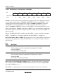
17.14.3 Erase Block Register 1 (EBR1)
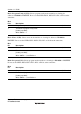
Bit : 7 6 5 4 3 2 1 0
EBR1 EB7 EB6 EB5 EB4 EB3 EB2 EB1 EB0
Initial value : 0 0 0 0 0 0 0 0
R/W : R/W R/W R/W R/W R/W R/W R/W R/W
EBR1 is an 8-bit register that specifies the flash memory erase area block by block. EBR1 is
initialized to H'00 by a reset, in hardware standby mode and software standby mode, and the
SWE1 bit in FLMCR1 is not set. When a bit in EBR1 is set, the corresponding block can be
erased. Other blocks are erase-protected. Set only one bit in EBR1 and EBR2 together (setting
more than one bit will automatically clear all EBR1 and EBR2 bits to 0). When on-chip flash
memory is disabled, a read will return H'00 and writes are invalid.
The flash memory block configuration is shown in table 17.28.