
Datasheet


Section 17 ROM
Rev.7.00 Feb. 14, 2007 page 638 of 1108
REJ09B0089-0700
17.13.9 Register Configuration
The registers used to control the on-chip flash memory when enabled are shown in table 17.27.
In order to access the FLMCR1, FLMCR2, EBR1, and EBR2 registers, the FLSHE bit must be set
to 1 in SYSCR2 (except RAMER).
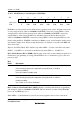
Table 17.27 Flash Memory Registers
Register Name Abbreviation R/W Initial Value Address
*
1
Flash memory control register 1 FLMCR1
*
6
R/W
*
3
H'80 H'FFC8
*
2
Flash memory control register 2 FLMCR2
*
6
R/W
*
3
H'00 H'FFC9
*
2
Erase block register 1 EBR1
*
6
R/W
*
3
H'00
*
4
H'FFCA
*
2
Erase block register 2 EBR2
*
6
R/W
*
3
H'00
*
5
H'FFCB
*
2
System control register 2 SYSCR2
*
7
R/W H'00 H'FF42
RAM emulation register RAMER R/W H'00 H'FEDB
Notes: 1. Lower 16 bits of the address.
2. Flash memory. Registers selection is performed by the FLSHE bit in system control
register 2 (SYSCR2).
3. In modes in which the on-chip flash memory is disabled, a read will return H'00, and
writes are invalid.
4. If a high level is input and the SWE bit in FLMCR1 is not set, these registers are
initialized to H'00.
5. Bits 3 to 0 are initialized to 0 when the SWE1 bit in FLMCR1 is not set, and bits 7 to 4
are initialized to 0 when the SWE2 bit in FLMCR2 is not set.
6. FLMCR1, FLMCR2, EBR1, and EBR2 are 8-bit registers. Only byte accesses are valid
for these registers, the access requiring 2 states.
7. The SYSCR2 register can only be used in the F-ZTAT version. In the mask ROM
version this register will return an undefined value if read, and cannot be modified.