
Datasheet


Section 17 ROM
Rev.7.00 Feb. 14, 2007 page 604 of 1108
REJ09B0089-0700
• When a bus master other than the CPU (the DTC) has control of the bus during
programming/erasing
Error protection is released only by a reset and in hardware standby mode.
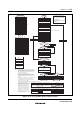
Figure 17.17 shows the flash memory state transition diagram.
RD VF PR ER
FLER = 0
Error
occurrence
RES = 0 or STBY = 0
RES = 0 or
STBY = 0
RD VF PR ER
FLER = 0
Normal operating mode
Program mode
Erase mode
Reset or hardware standby
(hardware protection)
RD VF PR ER
FLER = 1
RD VF PR ER
FLER = 1
Error protection mode
Error protection mode
(software standby)
Software
standby mode
FLMCR1, FLMCR2 (except FLER
bit), EBR1, EBR2 initialization state
FLMCR1, FLMCR2,
EBR1, EBR2
initialization state
Software standby
mode release
RD: Memory read possible
VF: Verify-read possible
PR: Programming possible
ER: Erasing possible
RD: Memory read not possible
VF: Verify-read not possible
PR: Programming not possible
ER: Erasing not possible
Legend:
RES = 0 or
STBY = 0
Error occurrence
(software standby)
Figure 17.17 Flash Memory State Transitions