
Datasheet


Section 17 ROM
Rev.7.00 Feb. 14, 2007 page 601 of 1108
REJ09B0089-0700
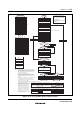
End of erasing
Start
Set SWE bit in FLMCR1
Set ESU bit in FLMCR1
Set E bit in FLMCR1
Wait (x) μs
Wait (y) μs
n = 1
Set EBR1, EBR2
Enable WDT
*2
*2
*4
Wait (z) ms
*2
Wait (α) μs
*2
Wait (β) μs
*2
Wait (γ) μs
Set block start address to verify address
*2
Wait (ε) μs
*2
*3
*2
Wait (η) μs
*2
*2
*5
Start of erase
Clear E bit in FLMCR1
Clear ESU bit in FLMCR1
Set EV bit in FLMCR1
H'FF dummy write to verify address
Read verify data
Clear EV bit in FLMCR1
Wait (η) μs
Clear EV bit in FLMCR1
Clear SWE bit in FLMCR1
Disable WDT
Halt erase
*1
Verify data = all 1?
Last address of block?
End of
erasing of all erase
blocks?
Erase failure
Clear SWE bit in FLMCR1
n ≥ N?
NG
NG
NG
NG
OK
OK
OK
OK
n ← n + 1
Increment
address
Notes: 1. Prewriting (setting erase block data to all 0) is not necessary.
2. The values of x, y, z, α, β, γ, ε, η, θ, and N are shown in section 20.3.6, Flash Memory Characteristics.
3. Verify data is read in 16-bit (W) units.
4. Set only one bit in EBR1or EBR2. More than one bit cannot be set.
5. Erasing is performed in block units. To erase a number of blo
cks, the individual blocks must be erased sequentially.
Wait (θ) μs Wait (θ) μs
Figure 17.16 Erase/Erase-Verify Flowchart