
Datasheet


Section 17 ROM
Rev.7.00 Feb. 14, 2007 page 599 of 1108
REJ09B0089-0700
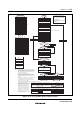
Start
End of programming
End sub
Set SWE bit in FLMCR1
Wait (x) μs
n = 1
m = 0
Sub-routine-call
See Note *7 for pulse width
Note: 7. Write Pulse Width
Start of programming
Sub-routine write pulse
Set PSU bit in FLMCR1
Enable WDT
Set P bit in FLMCR1
Wait (y) μs
Clear P bit in FLMCR1
Wait (z1) μs or (z2) μs or (z3) μs
Clear PSU bit in FLMCR1
Wait (α) μs
Disable WDT
Wait (β) μs
Write pulse application subroutine
NG
NG
NG
NG
NG NG
OK
OK
OK
OK
OK
Wait (γ) μs
Wait (ε) μs
*2
*4
*6
*6
*6
*6
*6
*6
*6
*6 *6
*5 *6
*6
*6
*6
*6
*1
Set PV bit in FLMCR1
H'FF dummy write to verify address
Read verify data
Additional program data computation
Transfer additional program data to
additional program data area
Read data = verify
data?
*4
*1
*4
*3
Reprogram data computation
Clear PV bit in FLMCR1
Clear SWE bit in FLMCR1
m = 1
128-byte
data verification
completed?
m = 0?
6 ≥ n ?
6 ≥ n ?
Increment address
Programming failure
OK
Clear SWE bit in FLMCR1
n ≥ N?
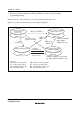
Reprogram Data (X')
0
1
Verify Data (V)
0
1
0
1
Additional Program Data (Y)
0
1
Comments
Additional programming executed
Additional programming not executed
Additional programming not ex
ecuted
Additional programming not executed
Additional Program Data Operation Chart
Write 128-byte data in RAM reprogram
data area consecutively to flash memory
Write pulse
(z1) μs or (z2) μs
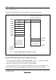
RAM
Program data area
(128 bytes)
Reprogram data area
(128 bytes)
Additional program data
area (128 bytes)
Store 128-byte program data in program
data area and reprogram data area
Number of Writes (n)
1
2
3
4
5
6
7
8
9
10
11
12
13
.
.
.
998
999
1000
Write Time (z) μs
z1
z1
z1
z1
z1
z1
z2
z2
z2
z2
z2
z2
z2
.
.
.
z2
z2
z2
Notes: 1. Data transfer is performed by byte transfer. The lower 8
bits of the first address written to must be H'00 or H'80. A
128-byte data transfer must be performed even if writing
fewer t
han 128 bytes; in this case, H'FF data must be
written to the extra addresses.
2. Verify data is read in 16-bit (W) units.
3. Even bits for which programming has been completed in
the
128-byte programming loop will be subjected to
additional programming if they fail the subsequent verify
operation.
4. A 128-byte area for storing program data, a 128-byte area
for storing reprogram data, and
a 128-byte area for
storing additional program data should be provided in
RAM. The contents of the reprogram
data and additional program data areas
are modified as programming proceeds.
5. A write pul
se of (z1) or (z2) ms should
be applied according to the progress of
programming. See note 7 for the pulse
widths. When the additional program
data is programmed, a
write pulse of
(z3) μs should be applied. Reprogram
data X' stands for reprogram data to
which a write pulse has been applied.
6. For the values of x, y, z1, z2, z3, α, β, γ,
ε, η, θ, and N,
see section 20.3.6, Flash
Memory Characteristics.
Original Data (D)
0
1
Verify Data (V)
0
1
0
1
Reprogram Data (X)
1
0
1
Comments
Programming completed
Programming incomplete; reprogram
Still in erased
state; no action
Program Data Operation Chart
Transfer reprogram data to reprogram
data area
n ← n + 1
Note: Use a (z3) μs write pulse for additional
programming.
Sequentially write 128-byte data in
additi
onal program data area in RAM to
flash memory
Write Pulse
(z3) μs additional write pulse
Wait (θ) μs
Wait (η) μs
Wait (θ) μs
Perform programming in
the erased state.
Do not perform additional
programming
on previously programmed
addresses.
Figure 17.15 Program/Program-Verify Flowchart