
Datasheet


Section 1 Overview
Rev.7.00 Feb. 14, 2007 page 23 of 1108
REJ09B0089-0700
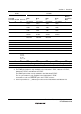
Pin No.
Type Symbol
TFP-100B,
TFP-100G
FP-100A TLP-113V I/O Name and Function
Watchdog
timer (WDT)
WDTOVF
*
6
60 62 G9 Output Watchdog timer overflows: The
counter overflows signal output pin in
watchdog timer mode.
TxD1,
TxD0
9, 8 11, 10 E4, E1 Output Transmit data (channel 0, 1):
Data output pins.
RxD1,
RxD0
11, 10 13, 12 E2, E3 Input Receive data (channel 0, 1):
Data input pins.
Serial com-
munication
interface
(SCI) Smart
Card
interface
SCK1
SCK0
13, 12 15, 14 F1, F4 I/O Serial clock (channel 0, 1):
Clock I/O pins.
A/D
converter
AN7 to
AN0
86 to 79 88 to 81 D7, C7, A7,
B8, C8, B9,
A8, D9
Input Analog 7 to 0: Analog input pins.
ADTRG 93 95 C6 Input A/D conversion external trigger input:
Pin for input of an external trigger to
start A/D conversion.
D/A
converter
DA1, DA0 86, 85 88, 87 D7, C7 Output Analog output: D/A converter analog
output pins.
A/D
converter
and D/A
converter
AV
CC
77 79 A11 Input This is the power supply pin for the
A/D converter and D/A converter.
When the A/D converter and D/A
converter are not used, this pin should
be connected to the system power
supply (V
CC
).
AV
SS
87 89 B7 Input This is the ground pin for the A/D
converter and D/A converter.
This pin should be connected to the
system power supply (0 V).
V
ref
78 80 A9 Input This is the reference voltage input pin
for the A/D converter and D/A
converter.
When the A/D converter and D/A
converter are not used, this pin should
be connected to the system power
supply (V
CC
).