
Datasheet


Section 1 Overview
Rev.7.00 Feb. 14, 2007 page 18 of 1108
REJ09B0089-0700
1.3.3 Pin Functions
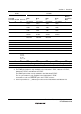
Table 1.3 Pin Functions
Pin No.
Type Symbol
TFP-100B,
TFP-100G
FP-100A TLP-113V I/O Name and Function
Power
supply
V
CC
40, 65,
98
42, 67,
100
B3, E11, L7 Input Power supply: For connection to the
power supply. All V
CC
pins should be
connected to the system power
supply.
V
SS
7, 18,
31, 49,
68, 88
9, 20,
33, 51,
70, 90
A6, D2, E9,
G3, J4, K3,
K10
Input Ground: For connection to ground
(0 V). All V
SS
pins should be
connected to the system power supply
(0 V).
Internal
voltage
step-down
pin
V
CL
*
1
60 62 G8 Output An external capacitor should be
connected between this pin and GND
(0 V). Do not connect it to V
CC
.
Clock XTAL 66 68 F10 Input Connects to a crystal oscillator.
See section 18, Clock Pulse
Generator, for typical connection
diagrams for a crystal oscillator and
external clock input.
EXTAL 67 69 F9 Input Connects to a crystal oscillator.
The EXTAL pin can also input an
external clock.
See section 18, Clock Pulse
Generator, for typical connection
diagrams for a crystal oscillator and
external clock input.
φ 69 71 D11 Output System clock: Supplies the system
clock to an external device.