
Datasheet


Section 11 Watchdog Timer
Rev.7.00 Feb. 14, 2007 page 417 of 1108
REJ09B0089-0700
11.1.3 Pin Configuration
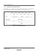
Table 11.1 describes the WDT output pin.
Table 11.1 WDT Pin
Name Symbol I/O Function
Watchdog timer overflow WDTOVF
*
Output Outputs counter overflow signal in watchdog
timer mode
Note: * The WDTOVF function is not available in the F-ZTAT versions.
11.1.4 Register Configuration
The WDT has three registers, as summarized in table 11.2. These registers control clock selection,
WDT mode switching, and the reset signal.
Table 11.2 WDT Registers
Address
*
1
Name Abbreviation R/W Initial Value Write
*
2
Read
Timer control/status register TCSR R/(W)
*
3
H'18 H'FFBC H'FFBC
Timer counter TCNT R/W H'00 H'FFBC H'FFBD
Reset control/status register RSTCSR R/(W)
*
3
H'1F H'FFBE H'FFBF
Notes: 1. Lower 16 bits of the address.
2. For details of write operations, see section 11.2.4, Notes on Register Access.
3. Only a write of 0 is permitted to bit 7, to clear the flag.