
Datasheet


Section 9 16-Bit Timer Pulse Unit (TPU)
Rev.7.00 Feb. 14, 2007 page 387 of 1108
REJ09B0089-0700
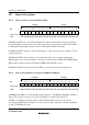
Contention between Buffer Register Write and Input Capture: If the input capture signal is
generated in the T
2
state of a buffer write cycle, the buffer operation takes precedence and the
write to the buffer register is not performed.
Figure 9.55 shows the timing in this case.
Input capture
signal
Write signal
A
ddress
φ
TCNT
Buffer register write cycle
T
1
T
2
N
TGR
N
M
M
Buffer
register
Buffer register
address
Figure 9.55 Contention between Buffer Register Write and Input Capture