
Datasheet


Section 9 16-Bit Timer Pulse Unit (TPU)
Rev.7.00 Feb. 14, 2007 page 384 of 1108
REJ09B0089-0700
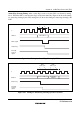
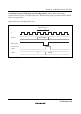
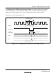
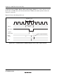
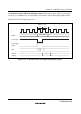
Contention between Buffer Register Write and Compare Match: If a compare match occurs in
the T
2
state of a TGR write cycle, the data transferred to TGR by the buffer operation will be the
data prior to the write.
Figure 9.52 shows the timing in this case.
Compare
match signal
Write signal
A
ddress
φ
Buffer register
address
Buffer
register
TGR write cycle
T
1
T
2
N
TGR
N M
Buffer register write data
Figure 9.52 Contention between Buffer Register Write and Compare Match