
Datasheet


Section 9 16-Bit Timer Pulse Unit (TPU)
Rev.7.00 Feb. 14, 2007 page 322 of 1108
REJ09B0089-0700
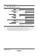
Channel
Bit 7
IOD3
Bit 6
IOD2
Bit 5
IOD1
Bit 4
IOD0
Description
3 0 0 0 0 Output disabled (Initial value)
1
0 output at compare match
1 0
1 output at compare match
1
TGR3D
is output
compare
register
*
2
Initial output is 0
output
Toggle output at compare
match
1 0 0 Output disabled
1 0 output at compare match
1 0
Initial output is 1
output
1 output at compare match
1
Toggle output at compare
match
1 0
0 0 Input capture at rising edge
1 Input capture at falling edge
1 ×
Capture input
source is
TIOCD3 pin
Input capture at both edges
1 × ×
TGR3D
is input
capture
register
*
2
Capture input
source is channel
4/count clock
Input capture at TCNT4
count-up/count-down
*
1
×: Don’t care
Notes: 1. When bits TPSC2 to TPSC0 in TCR4 are set to B'000 and φ/1 is used as the TCNT4
count clock, this setting is invalid and input capture is not generated.
2. When the BFB bit in TMDR3 is set to 1 and TGR3D is used as a buffer register, this
setting is invalid and input capture/output compare is not generated.