
Datasheet


Section 8 I/O Ports
Rev.7.00 Feb. 14, 2007 page 299 of 1108
REJ09B0089-0700
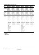
Pin Selection Method and Pin Functions
PG1/CS3/CS6/
IRQ7
The pin function is switched as shown below according to the combination of
operating mode and CSS36 bit in PFCR1, CS167E bit in PFCR2, CS25E bit
and bit PG1DDR.
Operating
Mode
Modes 4 to 6
*
1
Mode 7
*
1
PG1DDR 0 1 0 1
CS167E — 0 1 — —
CS25E — 0 1 0 1 — —
CSS36 — — 0 1 0 1 0 1 — —
Pin function PG1
input
pin
PG1
output
pin
CS3
output
pin
PG1 output
pin
CS6
output
pin
CS3
output
pin
CS6
output
pin
PG1
input
pin
PG1
output
pin
IRQ7 interrupt input pin
*
2
PG0/ADTRG/IRQ6 The pin function is switched as shown below according to the combination of
bits TRGS1 and TRGS0 (trigger select 1 and 0) in the A/D control register
(ADCR).
PG0DDR 0 1
Pin function PG0 input PG0 output
ADTRG input pin
*
3
IRQ6 interrupt input pin
*
2
Notes: 1. Modes 6 and 7 are not available in the ROMless versions.
2. When this pin is used as an external interrupt input, it should not be used as an
input/output pin with other functions.
3. ADTRG input when TRGS1 = TRGS0 = 1.