
Datasheet


Section 8 I/O Ports
Rev.7.00 Feb. 14, 2007 page 296 of 1108
REJ09B0089-0700
Port Function Control Register 1 (PFCR1)
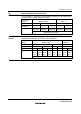
Bit : 7 6 5 4 3 2 1 0
CSS17 CSS36 PF1CS5S PF0CS4S A23E A22E A21E A20E
Initial value : 0 0 0 0 1 1 1 1
R/W : R/W R/W R/W R/W R/W R/W R/W R/W
PFCR1 is an 8-bit readable/writable register that performs I/O port control. PFCR1 is initialized to
H'0F by a reset, and in hardware standby mode.
Bit 7—CS17 Select (CSS17): Selects whether CS1 or CS7 is output from the PG3 pin. Change
the CSS17 bit setting only when the corresponding DDR bit is 0. This bit is valid in modes 4 to 6.
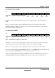
Bit 7
CSS17
Description
0 PG3 is the PG3/CS1 pin. CS1 output is enabled when CS167E = 1 and PG3DDR =
1 (Initial value)
1 PG3 is the PG3/CS7 pin. CS7 output is enabled when CS167E = 1 and PG3DDR =
1
Bit 6—CS36 Select (CSS36): Selects whether CS3 or CS6 is output from the PG1 pin. Change
the CSS36 bit setting only when the corresponding DDR bit is 0. This bit is valid in modes 4 to 6.
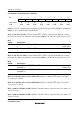
Bit 6
CSS36
Description
0 PG1 is the PG1/IRQ7/CS3 pin. CS3 output is enabled when CS25E = 1 and
PG1DDR = 1 (Initial value)
1 PG1 is the PG1/IRQ7/CS6 pin. CS6 output is enabled when CS167E = 1 and
PG1DDR = 1
Bit 5—Port F1 Chip Select 5 Select (PF1CS5S): Enables or disables CS5 output. For details,
see section 8.11, Port F.
Bit 4—Port F0 Chip Select 4 Select (PF0CS4S): Enables or disables CS4 output. For details,
see section 8.11, Port F.
Bit 3—Address 23 Enable (A23E): Enables or disables address output 23 (A23). For details, see
section 8.2, Port 1.
Bit 2—Address 22 Enable (A22E): Enables or disables address output 22 (A22). For details, see
section 8.2, Port 1.