
Datasheet


Section 8 I/O Ports
Rev.7.00 Feb. 14, 2007 page 245 of 1108
REJ09B0089-0700
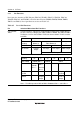
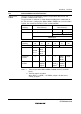
Pin Selection Method and Pin Functions
P20/TIOCA3 The pin function is switched as shown below according to the combination of
the TPU channel 3 setting by bits MD3 to MD0 in TMDR3, bits IOA3 to IOA0 in
TIOR3H, bits CCLR2 to CCLR0 in TCR3, and bit P20DDR.
TPU Channel
3 Setting
Table Below (1)
Table Below (2)
P20DDR — 0 1
Pin function TIOCA3 output P20 input P20 output
TIOCA3 input
*
1
TPU Channel
3 Setting
(2)
(1)
(2)
(1)
(1)
(2)
MD3 to MD0 B'0000 B'001× B'0010 B'0011
IOA3 to IOA0 B'0000
B'0100
B'1×××
B'0001 to
B'0011
B'0101 to
B'0111
B'××00 Other than B'××00
CCLR2 to
CCLR0
— — — — Other
than
B'001
B'001
Output
function
— Output
compare
output
— PWM
mode 1
output
*
2
PWM
mode 2
output
—
×: Don’t care
Notes: 1. TIOCA3 input when MD3 to MD0 = B'0000 and IOA3 to IOA0 =
B'10××.
2. TIOCB3 output is disabled.