
Datasheet


Section 8 I/O Ports
Rev.7.00 Feb. 14, 2007 page 232 of 1108
REJ09B0089-0700
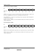
Pin Selection Method and Pin Functions
P12/TIOCC0/
TCLKA/A22
The pin function is switched as shown below according to the combination of
the operating mode, TPU channel 0 setting (by bits MD3 to MD0 in TMDR0,
bits IOC3 to IOC0 in TIOR0L, and bits CCLR2 to CCLR0 in TCR0), bits TPSC2
to TPSC0 in TCR0 to TCR5, bit A22E in PFCR1 and bit P12DDR.
Operating
Mode
Mode 7
*
1
Modes 4 to 6
*
1
TPU Channel
0 Setting
Table
Below (1)
Table
Below (2)
Table
Below (1)
Table
Below (2)
P12DDR — 0 1 0 1 0 1
A22E — — — — 0 1 — 0 1
Pin function TIOCC0
output
P12
input
P12
output
TIOCC0
output
TIOCC0
output
A22
output
P12
input
P12
output
A22
output
TIOCC0
input
*
2
TIOCC0
input
*
2
TCLKA input
*
3
TPU Channel
0 Setting
(2)
(1)
(2)
(1)
(1)
(2)
MD3 to MD0 B'0000 B'001× B'0010 B'0011
IOC3 to IOC0 B'0000
B'0100
B'1×××
B'0001 to
B'0011
B'0101 to
B'0111
B'××00 Other than B'××00
CCLR2 to
CCLR0
— — — — Other
than
B'101
B'101
Output
function
— Output
compare
output
— PWM
mode 1
output
*
4
PWM
mode 2
output
—
×: Don’t care
Notes: 1. Modes 6 and 7 are not available in the ROMless versions.
2. TIOCC0 input when MD3 to MD0 = B'0000 and IOC3 to IOC0 =
B'10××.
3. TCLKA input when the TCR0 to TCR5 setting is: TPSC2 to TPSC0
= B'100.
TCLKA input when channel 1 and 5 are set to phase counting
mode (MD3 to MD0 = B'01××).
4. TIOCD0 output is disabled.
When BFA = 1 or BFB = 1 in TMDR0, output is disabled and setting
(2) applies.