
Datasheet


Section 6 Bus Controller
Rev.7.00 Feb. 14, 2007 page 169 of 1108
REJ09B0089-0700
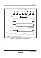
Figure 6.14 shows an example of wait state insertion timing.
By program wait
T
1
Address bus
φ
AS
RD
Data bus
Read data
Read
HWR, LWR
Write data
Write
Note: indicates the timing of WAIT pin sampling.
WAIT
Data bus
T
2
T
w
T
w
T
w
T
3
By WAIT pin
Figure 6.14 Example of Wait State Insertion Timing
The settings after a power-on reset are: 3-state access, 3 program wait state insertion, and WAIT
input disabled.