
Datasheet


Rev.7.00 Feb. 14, 2007 page ix of xxxii
REJ09B0089-0700
Item Page Revision (See Manual for Details)
12.2.8 Bit Rate
Register (BRR)
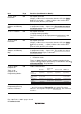
Table 12.3 BRR
Settings for Various
Bit Rates
(Asynchronous Mode)
452 Table 12.3 amended
φ = 25 MHz
Bit Rate
(bits/s) n N
Error
(%
)
110 3 110
–0.02
150 3 80
0.47
–0.15300 2 162
600 2 80
0.47
1200 1 162 –0.15
2400 1 80
0.47
4800 0 162 –0.15
9600 0 80
0.47
19200 0 40
–0.76
31250 0 24
0.00
38400 0 19
1.73
14.4.3 Input
Sampling and A/D
Conversion Time
Figure 14.5 A/D
Conversion Timing
545 Figure 14.5 amended
(1)
(2)
t
D
t
SPL
t
CONV
φ
Input sampling
timing
A
DF
Address bus
Write signal
17.4.1 Features 571 Description amended
• Reprogramming capability
The flash memory can be reprogrammed a minimum of 100
times.