
Datasheet


Appendix B Internal I/O Registers
Rev.7.00 Feb. 14, 2007 page 1046 of 1108
REJ09B0089-0700
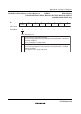
FCCS—Flash Code Control Status Register H'FFC4 FLASH
(Valid only in the H8S/2319C F-ZTAT)
7
⎯
1
R
6
⎯
0
R
5
⎯
0
R
4
FLER
0
R
3
⎯
0
R
0
SCO
0
(R)/W
2
⎯
0
R
1
⎯
0
R
Bit
Initial value
Read/Write
:
:
:
Flash Memory Error
0
1
Flash memory operates normally
Programming/erasing protection for flash memory
(error protection) is invalid.
[Clearing condition] At a power-on reset or in hardware
standby mode
Indicates an error occurs during programming/erasing
flash memory.
Programming/erasing protection for flash memory
(error protection) is valid.
[Setting condition] See section 17.25.3, Error Protection
Source Program Copy
Operation
0
1
Download of the on-chip programming/
erasing program to the on-chip RAM is
not executed
[Clearing condition] When download is
completed
Request that the on-chip programming/
erasing program i
s downloaded to the
on-chip RAM is occurred
[Setting conditions] When all of the
followingconditions are satisfied and 1 is
written to this bit
• FKEY is written to H'A5
• During execution i
n the on-chip RAM
• Not in RAM emulation mode (RAMS
in RAMER = 0)
Reserved bit
This bit is always read as 1.
The write value should always be 1.
Reserved bits
These bits are a
lways read as 0.
The write value should always be 0.
Reserved bits
These bits are always read as 0.
The write value should always be 0.