
Datasheet


Section 3 MCU Operating Modes
Rev.7.00 Feb. 14, 2007 page 74 of 1108
REJ09B0089-0700
only be used in modes 1 to 7. This means that the mode pins must be set to select one of these
modes.
Do not change the inputs at the mode pins during operation.
3.1.3 Register Configuration
The H8S/2319 Group has a mode control register (MDCR) that indicates the inputs at the mode
pins (MD2 to MD0), and a system control register (SYSCR) and system control register 2
(SYSCR2)
*
2
that control the operation of the chip. Table 3.3 summarizes these registers.
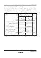
Table 3.3 Registers
Name Abbreviation R/W Initial Value Address
*
1
Mode control register MDCR R Undefined H'FF3B
System control register SYSCR R/W H'01 H'FF39
System control register 2
*
2
SYSCR2 R/W H'00 H'FF42
Notes: 1. Lower 16 bits of the address.
2. The SYSCR2 register can only be used in the F-ZTAT versions. In the mask ROM and
ROMless versions this register will return an undefined value if read, and cannot be
modified.
3.2 Register Descriptions
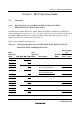
3.2.1 Mode Control Register (MDCR)
Bit : 7 6 5 4 3 2 1 0
— — — — — MDS2 MDS1 MDS0
Initial value : 1 0 0 0 0 —
*
—
*
—
*
R/W : — — — — — R R R
Note: * Determined by pins MD2 to MD0.
MDCR is an 8-bit read-only register that indicates the current operating mode of the H8S/2319
Group chip.
Bit 7—Reserved: This bit is always read as 1, and cannot be modified.
Bits 6 to 3—Reserved: These bits are always read as 0, and cannot be modified.