
Datasheet


Appendix B Internal I/O Registers
Rev.7.00 Feb. 14, 2007 page 1015 of 1108
REJ09B0089-0700
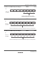
SCR0—Serial Control Register 0 H'FF7A SCI0
7
TIE
0
R/W
6
RIE
0
R/W
5
TE
0
R/W
4
RE
0
R/W
3
MPIE
0
R/W
0
CKE0
0
R/W
2
TEIE
0
R/W
1
CKE1
0
R/W
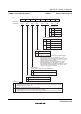
1
0 Asynchronous
mode
Internal clock/SCK pin functions
as I/O port
Clock Enable
0
1
Transmit-end interrupt (TEI) request disabled
*
Transmit-end interrupt (TEI) request enabled
*
Transmit End Interrupt Enable
0 Multiprocessor interrupts disabled
[Clearing conditions]
· When the MPIE bit is cleared to 0
· When data with MPB = 1 is received
Multiprocessor Interrupt Enable
0
1
Reception disabled
*
1
Reception enabled
*
2
Receive Enable
0
1
Transmission disabled
*
1
Transmission enabled
*
2
Transmit Enable
0 Receive-data-full interrupt (RXI) request and receive-error interrupt (ERI) request disabled
*
Receive Interrupt Enable
0
1
Transmit-data-empty interrupt (TXI) request disabled
*
Transmit-data-empty interrupt (TXI) request enabled
Transmit Interrupt Enable
Bit
Initial value
Read/Write
:
:
:
Synchronous
mode
Internal clock/SCK pin functions
as serial clock output
Asynchronous
mode
Internal clock/SCK pin functions
as clock output
*
1
Synchronous
mode
Internal clock/SCK pin functions
as serial clock output
Asynchronous
mode
External clock/SCK pin functions
as clock input
*
2
Synchronous
mode
External clock/SCK pin functions
as serial clock input
Asynchronous
mode
External clock/SCK pin functions
as clock input
*
2
Synchronous
mode
External clock/SCK pin functions
as serial clock input
Multiprocessor interrupts enabled
*
Receive-data-full interrupt (RXI) requests, receive-error interrupt (ERI) requests, and setting
of the RDRF, FER, and ORER flags in SSR are disabled until data with the multiprocessor bit
set to 1 is received
1
1 Receive-data-full interrupt (RXI) request and receive-error interrupt (ERI) request enabled
1
0
1
0
Notes: 1. Outputs a clock of the same frequency as the bit rate.
2. Inputs a clock with a frequency 16 times the bit rate.
Notes: 1. Clearing the RE bit to 0 does not affect the RDRF, FER, PER, and ORER flags, which retain their states.
2. Serial reception is started in this state when a start bit is detected in asynchronous mode or serial clock
input is detected in synchronous mode.
SMR setting must be performed to decide the receive format before setting the RE bit to 1.
Notes: 1. The TDRE flag in SSR is fixed at 1.
2. In this state, serial transmission is started when transmit data is written to TDR and the
TDRE flag in SSR is cleared to 0.
SMR setting must be performed to decide the transmit format before setting the TE bit to 1.
Note: * TEI clearing can be performed by reading 1 from the TDRE flag in SSR, then
clearing it to 0 and clearing the TEND flag to 0, or by clearing the TEIE bit to 0.
Note: * When receive data including MPB = 0 is received, receive data transfer from RSR to RDR,
receive error detection, and setting of the RDRF, FER, and ORER flags in SSR, is not
performed. When receive data including MPB = 1 is received, the MPB bit in SSR is set to 1,
the MPIE bit is cleared to 0 automatically, and generation of RXI and ERI interrupts (when
the TIE and RIE bits in SCR are set to 1) and FER and ORER flag setting is enabled.
Note: * RXI and ERI interrupt requests can be cleared by reading 1 from the RDRF, FER, PER, or
ORER flag, then clearing the flag to 0, or by clearing the RIE bit to 0.
Note: * TXI interrupt requests can be cleared by reading 1 from the
TDRE flag, then clearing it to 0, or by clearing the TIE bit to 0.