
Datasheet


Section 17 ROM
Rev.7.00 Feb. 14, 2007 page 715 of 1108
REJ09B0089-0700
(b) Flash pass/fail parameter (FPFR: general register R0L of CPU)
An explanation of FPFR as the return value indicating the erase result is provided here.
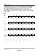
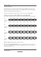
Bit : 7 6 5 4 3 2 1 0
0 MD EE FK EB 0 0 SF
Initial value : — — — — — — — —
R/W : — R/W R/W R/W R/W — — R/W
Bit 7—Reserved: Returns 0.
Bit 6—Erasure Mode Related Setting Error Detect (MD): Returns the check result of whether
the error protection state has been entered.
If the error protection state has been entered, 1 is written to this bit. This state can be confirmed by
checking bit 4, FLER, in the FCCS register. For conditions to enter the error protection state, see
section 17.25.3, Error Protection.
Bit 6
MD Description
0 FLER settings is normal (FLER = 0)
1 FLER = 1, and erasure cannot be performed
Bit 5—Erasure Execution Error Detect (EE): 1 is returned to this bit when the user MAT could
not be erased.
If this bit is set to 1, there is a high possibility that the user MAT is partially erased. In this case,
after removing the error factor, erase the user MAT.
If FMATS is set to H'AA and the user boot MAT is selected, an error occurs when erasure is
performed. In this case, both the user MAT and user boot MAT are not erased.
Erasing of the user boot MAT should be performed in the boot mode or PROM mode.
Bit 5
EE Description
0 Erasure has ended normally
1 Erasure has ended abnormally (erasure result is not guaranteed)