
Datasheet


Section 17 ROM
Rev.7.00 Feb. 14, 2007 page 676 of 1108
REJ09B0089-0700
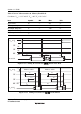
Table 17.39 AC Characteristics in Memory Read Mode
Conditions: V
CC
= 3.3 V ±0.3 V, V
SS
= 0 V, T
a
= 25°C ±5°C
Item Symbol Min Max Unit
Access time t
acc
— 20 μs
CE output delay time t
ce
— 150 ns
OE output delay time t
oe
— 150 ns
Output disable delay time t
df
— 100 ns
Data output hold time t
oh
5 — ns
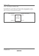
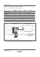
CE
A
18
to A
0
I/O
7
to I/O
0
OE
WE
VIH
VIL
VIL
t
acc
t
oh
t
oh
t
acc
Address stable Address stable
Figure 17.54 Timing Waveforms for CE/OE Enable State Read
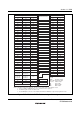
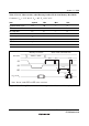
CE
A
18
to A
0
I/O
7
to I/O
0
VIH
OE
WE
t
ce
t
acc
t
oe
t
oh
t
oh
t
df
t
ce
t
acc
t
oe
Address stable Address stable
t
df
Figure 17.55 Timing Waveforms for CE/OE Clocked Read