
Datasheet


Section 17 ROM
Rev.7.00 Feb. 14, 2007 page 674 of 1108
REJ09B0089-0700
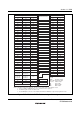
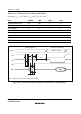
Table 17.37 AC Characteristics in Memory Read Mode
Conditions: V
CC
= 3.3 V ±0.3 V, V
SS
= 0 V, T
a
= 25°C ±5°C
Item Symbol Min Max Unit
Command write cycle t
nxtc
20 — μs
CE hold time t
ceh
0 — ns
CE setup time t
ces
0 — ns
Data hold time t
dh
50 — ns
Data setup time t
ds
50 — ns
Write pulse width t
wep
70 — ns
WE rise time t
r
— 30 ns
WE fall time t
f
— 30 ns
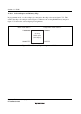
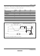
CE
A
18 to A
0
Data H'00
OE
WE
Command write
t
wep
t
ceh
t
dh
t
ds
t
f
t
r
t
nxtc
Note: Data is latched at the rising edge of WE.
t
ces
Memory read mode
Address stable
Data
Figure 17.52 Memory Read Mode Timing Waveforms after Command Write