
Datasheet


Section 17 ROM
Rev.7.00 Feb. 14, 2007 page 585 of 1108
REJ09B0089-0700
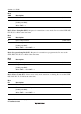
17.5.3 Erase Block Register 1 (EBR1)
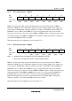
Bit : 7 6 5 4 3 2 1 0
EBR1 EB7 EB6 EB5 EB4 EB3 EB2 EB1 EB0
Initial value : 0 0 0 0 0 0 0 0
R/W : R/W R/W R/W R/W R/W R/W R/W R/W
EBR1 is an 8-bit register that specifies the flash memory erase area block by block. EBR1 is
initialized to H'00 by a reset, in hardware standby mode and software standby mode, when a low
level is input to the FWE pin, and when a high level is input to the FWE pin and the SWE bit in
FLMCR1 is not set. When a bit in EBR1 is set, the corresponding block can be erased. Other
blocks are erase-protected. Set only one bit in EBR1 and EBR2 together (setting more than one bit
will automatically clear all EBR1 and EBR2 bits to 0). When on-chip flash memory is disabled, a
read will return H'00 and writes are invalid.
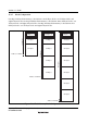
The flash memory block configuration is shown in table 17.7.
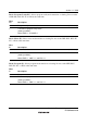
17.5.4 Erase Block Register 2 (EBR2)
Bit : 7 6 5 4 3 2 1 0
EBR2 — — EB13
*
1
EB12
*
1
EB11
*
2
EB10
*
2
EB9 EB8
Initial value : 0 0 0 0 0 0 0 0
R/W : — — R/W
*
1
R/W
*
1
R/W R/W R/W R/W
Notes: 1. Available only in the H8S/2315 F-ZTAT and H8S/2314 F-ZTAT.
2. Reserved in the H8S/2317 F-ZTAT. Only 0 should be written.
EBR2 is an 8-bit register that specifies the flash memory erase area block by block. EBR2 is
initialized to H'00 by a reset, in hardware standby mode and software standby mode, when a low
level is input to the FWE pin, and when a high level is input to the FWE pin and the SWE bit in
FLMCR1 is not set. When a bit in EBR2 is set, the corresponding block can be erased. Other
blocks are erase-protected. Set only one bit in EBR2 and EBR1 together (setting more than one bit
will automatically clear all EBR1 and EBR2 bits to 0, bits 7 to 2 are reserved in the H8S/2317
F-ZTAT). Bits 7 to 4 are reserved (bits 7 and 6 are reserved in the H8S/2315 F-ZTAT and
H8S/2314 F-ZTAT): they are always read as 0 and cannot be modified. When on-chip flash
memory is disabled, a read will return H'00, and writes are invalid.
The flash memory block configuration is shown in table 17.7.