
Datasheet


Section 8 I/O Ports
Rev.7.00 Feb. 14, 2007 page 272 of 1108
REJ09B0089-0700
8.9.2 Register Configuration
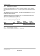
Table 8.15 shows the port D register configuration.
Table 8.15 Port D Registers
Name Abbreviation R/W Initial Value Address
*
Port D data direction register PDDDR W H'00 H'FEBC
Port D data register PDDR R/W H'00 H'FF6C
Port D register PORTD R Undefined H'FF5C
Port D MOS pull-up control register PDPCR R/W H'00 H'FF73
Note: * Lower 16 bits of the address.
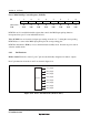
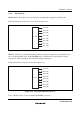
Port D Data Direction Register (PDDDR)
Bit : 7 6 5 4 3 2 1 0
PD7DDR PD6DDR PD5DDR PD4DDR PD3DDR PD2DDR PD1DDR PD0DDR
Initial value : 0 0 0 0 0 0 0 0
R/W : W W W W W W W W
PDDDR is an 8-bit write-only register, the individual bits of which specify input or output for the
pins of port D. PDDDR cannot be read; if it is, an undefined value will be read.
PDDDR is initialized to H'00 by a reset, and in hardware standby mode. It retains its prior state in
software standby mode.
• Modes 4 to 6
*
The input/output direction specification by PDDDR is ignored, and port D is automatically
designated for data I/O.
• Mode 7
*
Setting PDDDR bits to 1 makes the corresponding port D pins output ports, while clearing the
bits to 0 makes the pins input ports.
Note: * Modes 6 and 7 are not available in the ROMless versions.