
Datasheet


Section 6 Bus Controller
Rev.7.00 Feb. 14, 2007 page 156 of 1108
REJ09B0089-0700
6.3.5 Chip Select Signals
The chip can output chip select signals (CS0 to CS7) to areas 0 to 7, the signal being driven low
when the corresponding external space area is accessed.
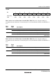
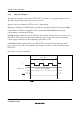
Figure 6.3 shows an example of CSn (n = 0 to 7) output timing.
Enabling or disabling of the CSn signal is performed by setting the data direction register (DDR),
CS167 Enable (CS167E), CS25 Enable, CSS17, CSS36, PF1CS5S, PF0CS4S for the port
corresponding to the particular CSn pin.
In ROM-disabled expansion mode, the CS0 pin is placed in the output state after a power-on reset.
Pins CS1 to CS7 are placed in the input state after a power-on reset, and so the corresponding
control registers should be set when outputting signals CS1 to CS7.
In the ROM-enabled expansion mode, pins CS0 to CS7 are all placed in the input state after a
power-on reset, and so the corresponding control registers should be set when outputting signals
CS0 to CS7.
For details, see section 8, I/O Ports.
Bus cycle
T
1
T
2
T
3
Area n external address
A
ddress bus
φ
CSn
Figure 6.3 CSn Signal Output Timing (n = 0 to 7)