
Datasheet


Section 6 Bus Controller
Rev.7.00 Feb. 14, 2007 page 141 of 1108
REJ09B0089-0700
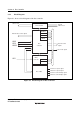
6.1.3 Pin Configuration
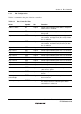
Table 6.1 summarizes the pins of the bus controller.
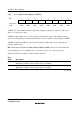
Table 6.1 Bus Controller Pins
Name Symbol I/O Function
Address strobe AS Output Strobe signal indicating that address output on
address bus is enabled.
Read RD Output Strobe signal indicating that external space is
being read.
High write HWR Output Strobe signal indicating that external space is
to be written, and upper half (D
15
to D
8
) of data
bus is enabled.
Low write LWR Output Strobe signal indicating that external space is
to be written, and lower half (D
7
to D
0
) of data
bus is enabled.
Chip select 0 CS0 Output Strobe signal indicating that area 0 is selected.
Chip select 1 CS1 Output Strobe signal indicating that area 1 is selected.
Chip select 2 CS2 Output Strobe signal indicating that area 2 is selected.
Chip select 3 CS3 Output Strobe signal indicating that area 3 is selected.
Chip select 4 CS4 Output Strobe signal indicating that area 4 is selected.
Chip select 5 CS5 Output Strobe signal indicating that area 5 is selected.
Chip select 6 CS6 Output Strobe signal indicating that area 6 is selected.
Chip select 7 CS7 Output Strobe signal indicating that area 7 is selected.
Wait WAIT Input Wait request signal when accessing external 3-
state access space.
Bus request BREQ Input Request signal that releases bus to external
device.
Bus request
acknowledge
BACK Output Acknowledge signal indicating that bus has
been released.
Bus request output BREQO Output External bus request signal used when internal
bus master accesses external space when
external bus is released.