
Datasheet


Section 2 CPU
Rev.7.00 Feb. 14, 2007 page 68 of 1108
REJ09B0089-0700
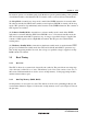
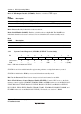
Internal address bus
Internal read signal
Internal data bus
Internal write signal
Internal data bus
φ
Bus cycle
T
1
Address
Read data
Write data
Read
access
Write
access
Figure 2.14 On-Chip Memory Access Cycle
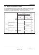
Bus cycle
T
1
Unchanged
A
ddress bus
AS
RD
HWR, LWR
Data bus
φ
High
High
High
High-impedance state
Figure 2.15 Pin States during On-Chip Memory Access