
Datasheet

Section 27 Electrical Characteristics
Rev. 6.00 Mar. 18, 2010 Page 881 of 982
REJ09B0054-0600
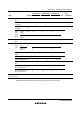
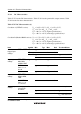
Condition A
Condition B Condition C
Item Symbol Min Max Min Max Min Max Unit
Test
Conditions
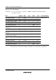
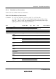
TMR Timer output delay
time
t
TMOD
⎯ 70 ⎯ 150 ⎯ 50 ns Figure 27.27
Timer reset input
setup time
t
TMRS
50 ⎯ 80 ⎯ 30 ⎯ ns Figure 27.29
Timer clock input
setup time
t
TMCS
50 ⎯ 80 ⎯ 30 ⎯ ns Figure 27.28
Single
edge
t
TMCWH
1.5 ⎯ 1.5 ⎯ 1.5 ⎯ t
cyc
Timer
clock
pulse
width
Both
edges
t
TMCWL
2.5 ⎯ 2.5 ⎯ 2.5 ⎯
WDT_1 BUZZ output delay
time
t
BUZD
⎯ 70 ⎯ 150 ⎯ 50 ns Figure 27.30
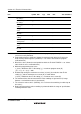
SCI
*
Asynchro-
nous
t
Scyc
4 ⎯ 4 ⎯ 4 ⎯ t
cyc
Figure 27.31
Input
clock
cycle
Synchro-
nous
6 ⎯ 6 ⎯ 6 ⎯
Input clock pulse
width
t
SCKW
0.4 0.6 0.4 0.6 0.4 0.6 t
Scyc
Input clock rise time t
SCKr
⎯ 1.5 ⎯ 1.5 ⎯ 1.5 t
cyc
Input clock fall time t
SCKf
⎯ 1.5 ⎯ 1.5 ⎯ 1.5
Transmit data delay
time
t
TXD
⎯ 75 ⎯ 150 ⎯ 50 ns Figure 27.32
Receive data setup
time (synchronous)
t
RXS
75 ⎯ 150 ⎯ 50 ⎯ ns
Receive data hold
time (synchronous)
t
RXH
75 ⎯ 150 ⎯ 50 ⎯ ns
A/D
converter
Trigger input setup
time
t
TRGS
40 ⎯ 60 ⎯ 30 ⎯ ns Figure 27.33
Note: * NMOS controls P35/SCK1 and P34 to output the high voltage. To output the high
voltage from P35/SCK1 and P34, connect an external pull-up resistor.