
Datasheet

Section 27 Electrical Characteristics
Rev. 6.00 Mar. 18, 2010 Page 871 of 982
REJ09B0054-0600
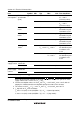
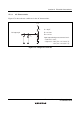
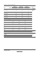
Table 27.15 Permissible Output Currents
Condition A (F-ZTAT version): V
CC
= 2.7 V to 3.6 V, AV
CC
= 2.7 V to 3.6 V,
V
ref
= 2.7 V to AV
CC
, V
SS
= AV
SS
= 0 V, T
a
= –20°C to
+75°C (regular specifications)
Condition B (Masked ROM version): V
CC
= 2.2 V to 3.6 V, AV
CC
= 2.2 V to 3.6 V,
V
ref
= 2.2 V to AV
CC
, V
SS
= AV
SS
= 0 V, T
a
= –20°C to
+75°C (regular specifications) T
a
= –40°C to +85°C (wide-
range specifications)
Condition C (F-ZTAT version): V
CC
= 3.0 V to 3.6 V, AV
CC
= 3.0 V to 3.6 V,
V
ref
= 3.0 V to AV
CC
, V
SS
= AV
SS
= 0 V, T
a
= –20°C to
+75°C (regular specifications), T
a
= –40°C to +85°C (wide-
range specifications)
Item Symbol Min Typ Max Unit
SCL1, SCL0,
SDA1, SDA0
V
CC
= 2.7 V to 3.6 V I
OL
⎯ ⎯ 10
V
CC
= 2.2 V to 3.6 V ⎯ ⎯ 0.5
Permissible output
low current (per pin)
Output pins
other than
above ones
V
CC
= 2.7 V to 3.6 V
I
OL
⎯ ⎯ 1.0
mA
V
CC
= 2.2 V to 3.6 V ⎯ ⎯ 30 Permissible output
low current (total)
Total of all
output pins
V
CC
= 2.7 V to 3.6 V
∑ I
OL
⎯ ⎯ 60
mA
V
CC
= 2.2 V to 3.6 V ⎯ ⎯ 0.5 Permissible output
high current (per pin)
All output pins
V
CC
= 2.7 V to 3.6 V
–I
OH
⎯ ⎯ 1.0
mA
V
CC
= 2.2 V to 3.6 V ⎯ ⎯ 15 Permissible output
high current (total)
Total of all
output pins
V
CC
= 2.7 V to 3.6 V
∑ –I
OH
⎯ ⎯ 30
mA
Note: To protect chip reliability, do not exceed the output current values in table 27.15.