
Datasheet


Section 27 Electrical Characteristics
Rev. 6.00 Mar. 18, 2010 Page 866 of 982
REJ09B0054-0600
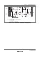
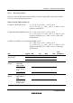
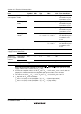
Item
Symbol
Min
Typ
Max
Unit
Test
Conditions
V
OH
V
CC
– 0.5 ⎯ ⎯ V I
OH
= –200 µA Output high
voltage
All output
pins
*
4
except
P34 and P35
V
CC
– 1.0 ⎯ ⎯ V I
OH
= –1 mA
*
2
P34 and P35
*
3
V
CC
– 2.0 ⎯ ⎯ V
I
OH
= –100 µA
(reference
value)
⎯ ⎯ 0.4 V I
OL
= 0.4 mA
Output low
voltage
All output
pins
*
4
V
OL
⎯ ⎯ 0.4 V I
OL
= 0.8 mA
*
2
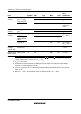
RES ⎯ ⎯ 1.0 µA
Input leakage
current
STBY, NMI,
FWE, MD2 to
MD0
⎯ ⎯ 1.0 µA
V
in
= 0.2 to
V
CC
– 0.2 V
Ports 4, 9
| I
in
|
⎯ ⎯ 1.0 µA
V
in
= 0.2 to
AV
CC
– 0.2 V
Three states
leakage
current (off)
Ports 1, 3, 7,
and A to G
| I
TSI
| ⎯ ⎯ 1.0 µA
V
in
= 0.2 to V
CC
– 0.2 V
Input pull-up
MOS current
Ports A to E –I
P
10 ⎯ 300 µA V
in
= 0V
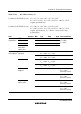
Notes: 1. If the A/D or D/A converter is not used, the AV
CC
, V
ref
, and AV
SS
pins should not be open.
Even if the A/D or D/A converter is not used, connect the AV
CC
and V
ref
pins to V
CC
and
supply 2.0 V to 3.6 V. In this case, V
ref
≤ AV
CC
.
2. V
CC
= 2.7 V to 3.6 V
3. P35/SCK1 and P34 function as NMOS push-pull output. To output the high voltage,
connect an external pull-up resistor.
4. In the case when ICE = 0. Low voltage output with bus driving function is specified in
table 27.16.
5. When V
CC
< AV
CC
, the maximum value for P40 and P41 is V
CC
+ 0.3 V.