
Datasheet


Section 11 16-Bit Timer Pulse Unit (TPU)
Rev. 6.00 Mar. 18, 2010 Page 433 of 982
REJ09B0054-0600
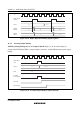
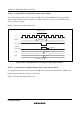
Interrupt
request
signal
Status flag
Address
Source address
DTC/DMAC
*
read cycle
T
1
T
2
Destination
address
T
1
T
2
DTC/DMAC
*
write cycle
φ
Note: * Supported only by the H8S/2239 Group.
Figure 11.44 Timing for Status Flag Clearing by DTC/DMAC* Activation
Note: * Supported only by the H8S/2239 Group.
11.10 Usage Notes
11.10.1 Module Stop Mode Setting
TPU operation can be disabled or enabled using the module stop control register. The initial
setting is for TPU operation to be halted. Register access is enabled by clearing module stop
mode. For details, refer to section 24, Power-Down Modes.
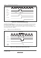
11.10.2 Input Clock Restrictions
The input clock pulse width must be at least 1.5 states in the case of single-edge detection, and at
least 2.5 states in the case of both-edge detection. The TPU will not operate properly with a
narrower pulse width.
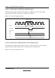
In phase counting mode, the phase difference and overlap between the two input clocks must be at
least 1.5 states, and the pulse width must be at least 2.5 states. Figure 11.45 shows the input clock
conditions in phase counting mode.