
Datasheet


Rev. 6.00 Mar. 18, 2010 Page xv of lx
REJ09B0054-0600
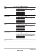
Item Page Revision (See Manual for Details)
16.3.6 I
2
C Bus Control
Register (ICCR)
644 Table amended
Bit
Bit Name
Initial
Value
R/W
Description
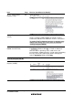
7 ICE 0 R/W I
2
C Bus Interface Enable
When this bit is set to 1, the I
2
C bus interface module is
enabled to send/receive data and drive the bus since it is
connected to the SCL and SDA pins. ICMR and ICDR can be
accessed.
SCL and SDA output is disabled (and input to SCL and SDA is
enabled) when this bit is cleared to 0. SAR and SARX can be
accessed.
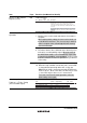
16.4.6 Slave Transmit
Operation
670 Description added
1. Initialize slave receive mode and wait for slave address
reception.
When making initial settings for slave receive mode, set
the ACKE bit in ICCR to 1. This is necessary in order to
enable reception of the acknowledge bit after entering
slave transmit mode.
Description amended
4. The master device drives SDA low at the 9th clock pulse,
and returns an acknowledge signal. When the value of
the ACKE bit in ICSR is 1, the acknowledge signal state
is stored in the ACKB bit, so the ACKB bit can be used to
determine whether the transfer operation was performed
successfully.
671 Description added
10. When the stop condition is detected, that is, when SDA
is changed from low to high when SCL is high, the
BBSY flag in ICCR is cleared to 0 and the STOP flag in
ICSR is set to 1. At the same time, the IRIC flag is set to
1. If the IRIC flag has been set, it is cleared to 0.
To restart slave transmit mode operation, make the
initial settings once again.
16.6 Usage Notes
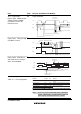
Table 16.7 I
2
C Bus Timing
(SCL and SDA Output)
677 Table amended
Item Symbol Output Timing Unit Notes
SCL output cycle time t
SCLO
28 t
cyc
to 256 t
cyc
ns
SCL output high pulse width t
SCLHO
0.5 t
SCLO
ns
SCL output low pulse width t
SCLLO
0.5 t
SCLO
ns
Figure 27.34