
User manual


Table Of Contents
- Notes regarding these materials
- Precautions on Using The Product Described Herein
- For Inquiries About Product Contents or This Manual
- Preface
- Contents
- 1. Overview
- 2. Contents of the Product Package
- 3. Usage Precautions
- 4. Starter Kit Usage Conditions
- 5. Hardware Setup
- 6. Software Setup
- Appendix 1 Contents of CD-ROM
- Appendix 2 Part List
- Appendix 3 M3A-2152G02 Product Standards
- 1. Overview
- 2. Functional Specifications
- 2.1 Configuration of the Power Supply
- 2.2 FP Select Circuit
- 2.3 MOD Select Circuit
- 2.4 Serial I/O Interface
- 2.5 Oscillator Circuit
- 2.6 General-purpose Output Port LED Indicators
- 2.7 General-purpose Input Port Control Circuit
- 2.8 Analog Port Input Control Circuit
- 2.9 CAN Interface
- 2.10 JTAG Peripheral Circuit
- 3. Reference Data
- REVISION HISTORY
32176 Group
Starter Kit User’s Manual M3A-2152
REJ10B0224-0300/Rev.3.00 Jan. 2007 Page 58 of 82
3. Reference Data
3.1 Jumper and Test Pin Lists
3.1.1 Jumpers
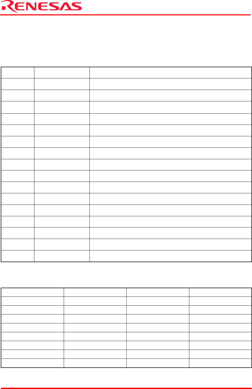
Table 3.1 Jumper List
Jumper No. Default Description
J1 Shorted between 1–4 Outputs a clock from X1 (surface mount-type oscillator module)
J2 Shorted between 1–2 Sets MOD1 to 0
J4 Shorted between 1–2
MOD0 is controled by EXTMOD0 or is set to 0 unless it is controled
by EXTMOD0
J5 Shorted between 1–2 Uses the CAN0 terminating resistor mounted on-board
J6 Shorted between 1–2 Enables reprogramming the M32R/ECU’s internal flash
J7 Shorted between 1–2 Uses the CAN1 terminating resistor mounted on-board
J9 Shorted between 1–2 Connects P83/RXD0 to the extension connector (CON2)
J10 Shorted between 1–2 Connects P86/RXD1 to the extension connector (CON2)
J11 Shorted between 1–2 Connects P175/RXD2 to the extension connector (CON2)
J12 Shorted between 1–2 Connects P75/RXD3 to the extension connector (CON1)
J13 Shorted between 1–2 Connects P221 to the extension connector (CON1)
J14 Shorted between 1–2 Connects P77 to the extension connector (CON1)
H1 Shorted between 1–2 Power supply from VCCE (CN2)
H3 Shorted between 1–2 Uses the VR control (VOL0)
H4 Shorted between 1–2 Uses the VR control (VOL1)
H6 Shorted between 1–2 Power supply from AVCC
3.1.2 Test Pins
Table 3.2 List of Test Pins
Test Pin No. Signal Name Test Pin No. Signal Name
TX1 AVCC TX10 CANL0
TX2 GND TX11 CANH1
TX3 GND TX12 CTX1
TX4 VCCE TX13 CRX1
TX6 MOD0 TX14 FP
TX7 CANH0 TX15 CANL21
TX8 CTX0 TX16 TXD1
TX9 CRX0 TX18 VREF0