
User manual


Table Of Contents
- Notes regarding these materials
- Precautions on Using The Product Described Herein
- For Inquiries About Product Contents or This Manual
- Preface
- Contents
- 1. Overview
- 2. Contents of the Product Package
- 3. Usage Precautions
- 4. Starter Kit Usage Conditions
- 5. Hardware Setup
- 6. Software Setup
- Appendix 1 Contents of CD-ROM
- Appendix 2 Part List
- Appendix 3 M3A-2152G02 Product Standards
- 1. Overview
- 2. Functional Specifications
- 2.1 Configuration of the Power Supply
- 2.2 FP Select Circuit
- 2.3 MOD Select Circuit
- 2.4 Serial I/O Interface
- 2.5 Oscillator Circuit
- 2.6 General-purpose Output Port LED Indicators
- 2.7 General-purpose Input Port Control Circuit
- 2.8 Analog Port Input Control Circuit
- 2.9 CAN Interface
- 2.10 JTAG Peripheral Circuit
- 3. Reference Data
- REVISION HISTORY
32176 Group
Starter Kit User’s Manual M3A-2152
REJ10B0224-0300/Rev.3.00 Jan. 2007 Page 51 of 82
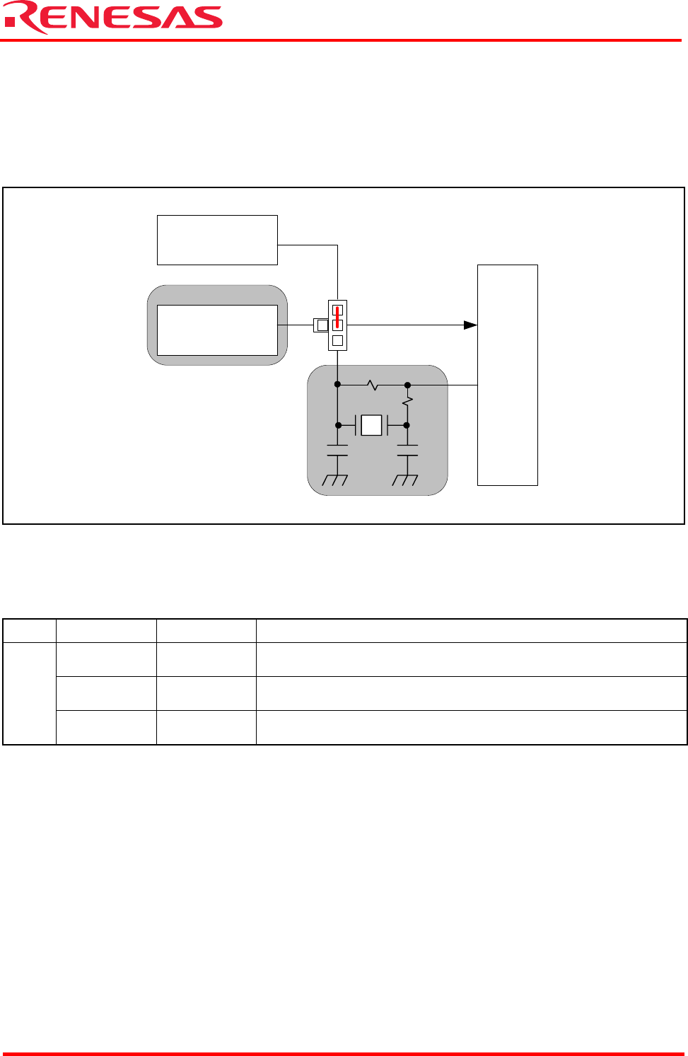
2.5 Oscillator Circuit
The oscillator circuit can be selected from three options by using the jumper J1: a surface
mount-type 10 MHz crystal oscillator module, a DIP-type crystal oscillator module or a crystal
resonator.
By default, the surface mount-type 10 MHz crystal oscillator module is selected.
Figure 2.5 Oscillator Circuit
Note: The shaded sections in the above diagram have only patterns available. When using the resonator Y1, please
be sure to add capacitors (C3, C4) and a resistor (R4).
Table 2.8 Oscillator Circuit Connections (Jumper)
Name Default Condition Description
{
Shorted
between 1–4
Outputs a clock from X1 (surface mount-type oscillator module)
Shorted
between 2–4
Outputs a clock from X2 (DIP-type oscillator module)
J1
Shorted
between 3–4
Outputs a clock from Y1 (resonator)
Note: The J1 jumper is shorted by soldering.
U1
M32R/ECU
XOUT
J1
1
2
X1
XINOUT
C3
R3
R4
Y1
X2
C4
OUT
3
4
Surface
mount-type
oscillator module
DIP-type
oscillator module