APPLICATION NOTE SH7145F Asynchronous Serial Data Transmission/Reception Summary The SH7144 series is a single-chip microprocessor based on the SH-2 RISC (Reduced Instruction Set Computer) CPU core and integrating a number of peripheral functions. This application note describes asynchronous serial data transmission/reception using the SCI (Serial Communication Interface) module of the SH7145F. It is intended to be used as reference by users designing software applications.
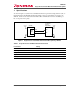
SH7145F Asynchronous Serial Data Transmission/Reception 1. Specifications As shown in figure 1, asynchronous serial data transmission is performed using channel 1 (ch1) of the SCI module of the SH7145F. In this task example 3 bytes of serial data are received by the SH7145, and the receive data is then transmitted. The communication format is 192,000 bps, 8bit, one stop bit, and no parity. 3.3 V Serial data transfer target MCU SH7145 TXD SCI (ch1) RXD 3.
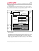
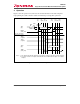
SH7145F Asynchronous Serial Data Transmission/Reception 2 Functions Used In this task example the SCI (Serial Communication Interface) is used to perform asynchronous serial data transmission/reception. Figure 2 shows a block diagram of channel 1 (ch1) of the SCI module. The functions of the elements shown in figure 2 are described below.
SH7145F Asynchronous Serial Data Transmission/Reception • On-Chip Peripheral Clock Pφ This is the reference clock for operation of on-chip peripheral functions. The clock signal is generated by a clock oscillator. • Receive Shift Register (RSR_1) This register is used to receive serial data. Serial data is input to RSR_1 from the RxD_1 pin. When one frame of data has been received, it is automatically transferred to the receive data register (RDR_1). RSR_1 cannot be accessed by the CPU.
SH7145F Asynchronous Serial Data Transmission/Reception • Bit Rate Register (BRR_1) This 8-bit register is used to adjust the bit rate. The SCI has independent baud rate generators for the individual channels, allowing different bit rates to be set for each. See the hardware manual for details on setting values, execution rate relationships, etc. Table 2 shows the function allocations for the task example.
SH7145F Asynchronous Serial Data Transmission/Reception 3. Operation Figure 3 shows the operation of asynchronous mode data transmission in the task example. To help explain figure 3, table 3 lists the software and hardware processing that is performed.
SH7145F Asynchronous Serial Data Transmission/Reception Table 3 Processing Software Processing Hardware Processing (1) — RSR_1 receives serial data and transfers it to RDR_1 (2) — Set RDRF flag in SSR_1 to 1 (3) Read data from RDR_1 (4) Clear RDRF flag in SSR_1 to 0 (5) Write receive data to TDR_1 — (6) Clear TDRE flag in SSR_1 to 1 — (7) — Transfer data from TDR_1 to TSR_1 (8) — Set TDRE flag in SSR_1 to 1 and output transmit data from pin TXD1 (9) — RSR_1 receives serial data an
SH7145F Asynchronous Serial Data Transmission/Reception 4. Software (1) Module Descriptions Table 4 lists the modules used in the task example. Table 4 Module Descriptions Module Label Function Main routine main Calls modules SCI routine init_sci Initial settings of SCI1 Receive routine rcv_sci Receives serial data Transmit routine trans_sci Transmits serial data Error handling err_int Handles receive errors (2) Argument Descriptions Table 5 lists the arguments used in the task example.
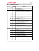
SH7145F Asynchronous Serial Data Transmission/Reception Table 6 On-Chip Register Descriptions Register Bit MSTCR1 MSTP17 Set Value 0 Function Module standby control register 1 SCI1 standby control bit Standby cancelled when MSTP17 = 0 SCR_1 H'70 Serial control register 1 (SCI_1) Transmit and receive control, interrupt control, transmit and receive clock source control TIE 0 RIE 1 Transmit interrupt enable TXI interrupt requests enabled when set to 1 Receive interrupt enable RXI and ERI interrup
SH7145F Asynchronous Serial Data Transmission/Reception Register Bit SMR_1 Set Value Function MP 0 Multiprocessor mode (enabled in asynchronous mode only) CKS1 0 Clock select 1, 0 CKS2 0 When value is 00, Pφ clock selected using on-chip baud rate generator as clock source Multiprocessor communication disabled when 0 BRR_1 H'40 Bit rate register 1 8-bit register for adjusting bit rate SDCR_1 H'F2 Serial direction control register 1 DIR bit (bit 3) selects LSB-first or MSB-first In task exam
SH7145F Asynchronous Serial Data Transmission/Reception 5. Flowcharts (1) Main Routine main() Initialize SCI module init_sci() rcv_sci() Receive 1st byte of data rcv_sci() Receive 2nd byte of data rcv_sci() Receive 3rd byte of data REJ06B0357-0100O/Rev.1.
SH7145F Asynchronous Serial Data Transmission/Reception (2) SCI1 Initialize Routine init_sci() Cancel SCI1 module standby status Clear to 0 bits TIE, RIE, TE, RE, MPIE, and TEIE in SCR_0 Select on-chip clock as clock source using CKE1 and CKE0 in SCR_0 Using SMR_1, select asynchronous mode, 8 data bits, no parity, 1 stop bit, and Pφ as baud rate generator clock source Using BRR_1, set communication speed to 19,200 bps Using DIR bit in SDCR_1, select LSB-first communication Wait minimum 1-bit transf
SH7145F Asynchronous Serial Data Transmission/Reception (3) Data Receive Routine rcv_sci() Wait until RDR_1 finishes receiving data No Yes Read receive data from RDR_1 and store it in on-chip RAM Clear RDRF flag in SSR_1 to 0 Transmit receive data without modification RTE (4) Data Transfer Routine trans_sci() Wait until possible to write to TDR_1 No Yes Write transmit data to TDR_1 Clear TDRE bit in SSR_1 to 0 RTE REJ06B0357-0100O/Rev.1.
SH7145F Asynchronous Serial Data Transmission/Reception 6. Program Listing /**************************************************************/ /* SH7145F Application Note */ /* */ /* Function */ /* :SCI1 */ /* */ /* External input clock : 12.5MHz */ /* Internal CPU clock : 50MHz */ /* Internal peripheral clock : 25MHz */ /* */ /* Written :2003/7 Rev.1.0 */ /**************************************************************/ #include "iodefine.h" #include
SH7145F Asynchronous Serial Data Transmission/Reception Function : init_sci Operation : Initialize serial (sci1) Asynchronous receive operation -Data : 8bit -Stop bit : 1bit -Parity bit : No **************************************************************/ void init_sci(void) { unsigned long i; P_STBY.MSTCR1.BIT.MSTP17 = 0; /* disable SCI1 standby mode /* Initialize SCI Asynchronous mode * P_SCI1.SCR_1.BYTE &= 0x03 ; /* P_SCI1.SCR_1.BIT.CKE = 0; /* P_SCI1.SMR_1.
SH7145F Asynchronous Serial Data Transmission/Reception P_SCI1.SSR_1.BIT.
SH7145F Asynchronous Serial Data Transmission/Reception Keep safety first in your circuit designs! 1. Renesas Technology Corp. puts the maximum effort into making semiconductor products better and more reliable, but there is always the possibility that trouble may occur with them. Trouble with semiconductors may lead to personal injury, fire or property damage.