
User's Manual
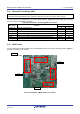
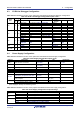
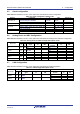
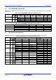
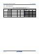
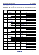
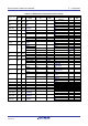
Table Of Contents
- 1. Overview
- 2. Power Supply
- 3. Board Layout
- 4. Connectivity
- 5. User Circuitry
- 6. Configuration
- 6.1 Modifying the RSSK
- 6.2 MCU Operating Modes
- 6.3 E1/E2 Lite Debugger Configuration
- 6.4 Power Supply Configuration
- 6.5 Clock Configuration
- 6.6 Analog Power and ADC Configuration
- 6.7 CAN Configuration
- 6.8 I2C & EEPROM Configuration
- 6.9 IRQ & Switch Configuration
- 6.10 LED Configuration
- 6.11 MCU Header Configuration
- 6.12 PMOD1 Configuration
- 6.13 PMOD2 Configuration
- 6.14 Bluetooth® Low Energy (BLE)
- 6.15 Serial Sound Interface (SSI)
- 6.16 Touch Interface Configuration
- 6.17 USB to Serial Configuration
- 6.18 USB Configuration
- 7. Code Development
- 8. Additional Information
- 9. Certification of Compliance
Renesas Solution Starter Kit for RX23W 6. Configuration
R20UT4446EG0102 Rev. 1.02 Page 24 of 41
Jun 22, 20
6.3 E1/E2 Lite Debugger Configuration
Table 6-2 below details the function of the option links associated with E1/E2 Lite Debugger Configuration.
Table 6-2: E1/E2 Lite Debugger Configuration Option Links
Signal
name
MCU
MCU Peripheral Selection
Destination Selection
Pin
Port
Signal
Fit DNF
Interface
/Function
Fit DNF
P26 B2 P26
PMOD1-MOSI
J7 (2-3pin short), R204
R62, R73, R205
PMOD1.2
-
-
EMU-TXD
J7 (2-3pin short), R62
R204, R73, R205
E1.5
-
-
SSIRXD0
J7 (2-3pin short), R73
R204, R62, R205
P26
-
-
SERIAL-TXD
J7 (2-3pin short), R205
R204, R62, R73
U8.2
-
R203
USB0-VBUSEN
J7 (1-2pin short)
-
U5.4
-
-
P30 A2 P30
PMOD1-MISO
J6 (2-3pin short)
R76, R80, R209
PMOD1.3
-
-
SW2
J6 (1-2pin short)
R76, R80, R209
SW2
-
-
EMU-RXD
R76
J6 (open), R80, R209
E1.11
-
-
AUDIO_MCLK
R80
J6 (open), R76, R209
P30
-
-
SERIAL-RXD
R209
J6 (open), R76, R80
U10. 2
-
R208
PC7 F1 PC7
EMU-UB
- -
E1.10
-
-
DSW-UB
SW3.2
-
-
PC7
-
-
PC7
-
-
SERIAL-TXD R203 - U8.2
J7 (1-2pin
short)
-
RESn B6 -
EMU-RESn
-
-
E1.13
-
-
SW-RESn
-
-
RES(Switch)
-
-
MD_FINED B7 -
EMU-MD_FINED
-
-
E1.7
-
-
DSW-MD_FINED
-
-
SW3.1
-
-
6.4 Power Supply Configuration
Table 6-3 below details the function of the option links associated with Power Supply Configuration.
Table 6-3: Power Supply Configuration Option Links
Reference
Configuration
Fit
DNF
Related Links
USB0_2 Connect 5V Power rail to VBUS0.
J3 (2-3 short),
J5 (1-2 short)
- U6.1, U6.2
USBCN0 Connect 5V Power rail to FT234_5V.
J3 (1-2 short),
J5 (1-2 short)
- U6.1, U6.2
USB_5V
Connect 5V power rail to USB_5V.
R57
-
U5.2, U5.3
U6 Output
Connect U6 Output power rail to Board_VCC.
J13 (short)
-
-
Board_5V
Connect 5V power rail to Board_5V.
-
-
U3.8, U6.1, U6.2
Board_VCC
Connect Board_VCC power rail to UC_VCC.
-
-
E1.8, U3.8
UC_VCC
Connect Board_VCC power rail to UC_VCC. J10 (short) - U1
Enable current probe for measurement MCU
current consumption.
- J10 (open) U1
VBATT
Connect UC_VCC power rail to VBATT.
R133
R134
U1
J11
*1
connected to VBATT of MCU .
R134
R133
U1
*1
: J11 is a power connector for VBATT, not a jumper. Do not short-circuit J11 Pin 1 and Pin 2 because the
power supply is directly connected to ground.
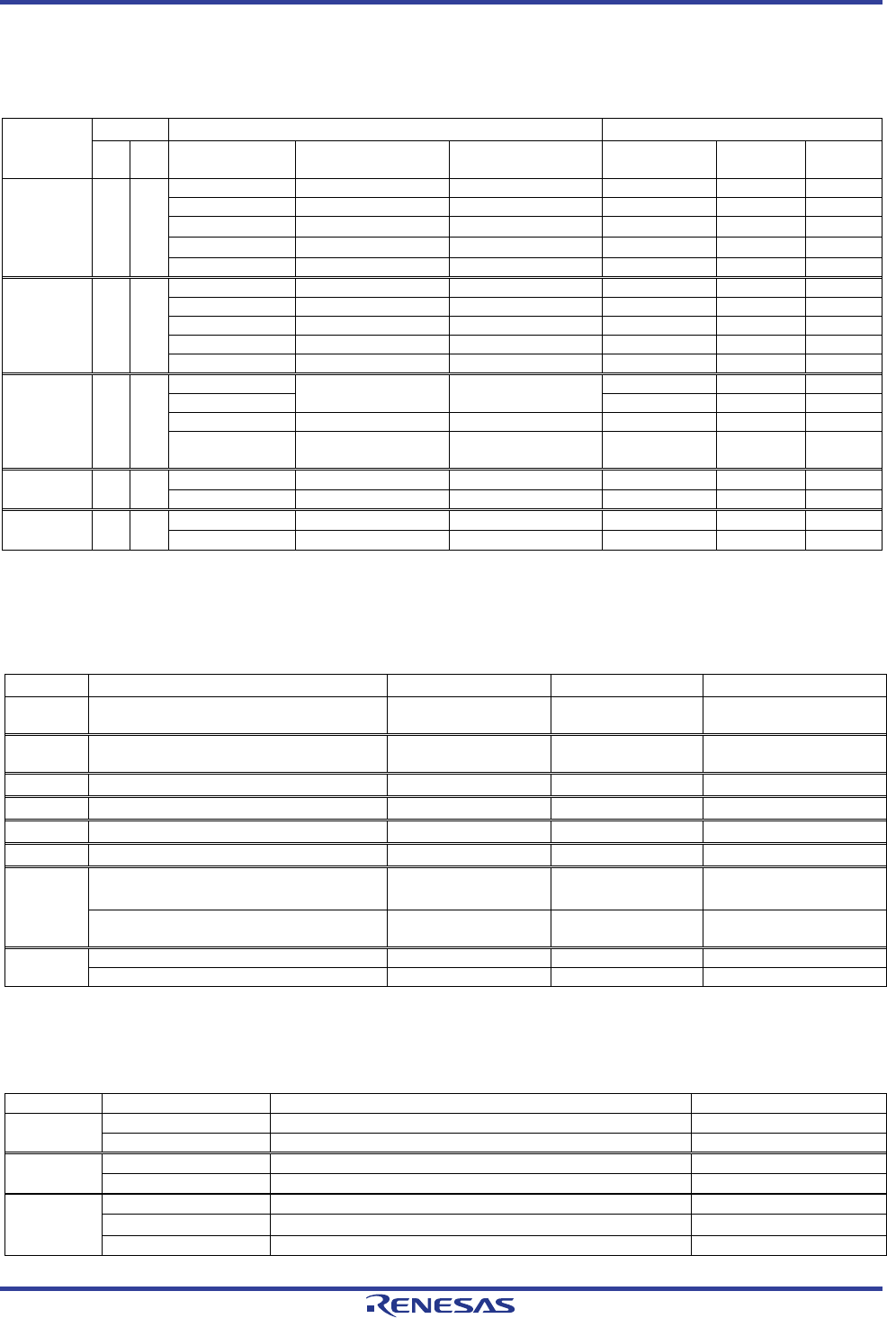
Table 6-4 below details the function of the jumpers associated with the Power Supply Configuration.
Table 6-4: Power Supply Configuration Jumper Settings
Reference
Jumper Position
Configuration
Related Links.
J10
Short
Connect Board_VCC power rail to UC_VCC.
-
Open
Enable current probe for measurement MCU current consumption.
-
J13
Short
Enable U6 Output power.
-
Open
Disable U6 Output power.
-
J3
1-2 Short
Enable USBCN0(FT234_5V).
-
2-3 Short
Enable USB0_2(VBUS0).
J5 (1-2 short)
All open
Disable USBCN0(FT234_5V), USB0_2(VBUS0).
-