
User's Manual
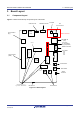
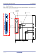
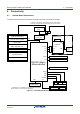
Table Of Contents
- 1. Overview
- 2. Power Supply
- 3. Board Layout
- 4. Connectivity
- 5. User Circuitry
- 6. Configuration
- 6.1 Modifying the RSSK
- 6.2 MCU Operating Modes
- 6.3 E1/E2 Lite Debugger Configuration
- 6.4 Power Supply Configuration
- 6.5 Clock Configuration
- 6.6 Analog Power and ADC Configuration
- 6.7 CAN Configuration
- 6.8 I2C & EEPROM Configuration
- 6.9 IRQ & Switch Configuration
- 6.10 LED Configuration
- 6.11 MCU Header Configuration
- 6.12 PMOD1 Configuration
- 6.13 PMOD2 Configuration
- 6.14 Bluetooth® Low Energy (BLE)
- 6.15 Serial Sound Interface (SSI)
- 6.16 Touch Interface Configuration
- 6.17 USB to Serial Configuration
- 6.18 USB Configuration
- 7. Code Development
- 8. Additional Information
- 9. Certification of Compliance
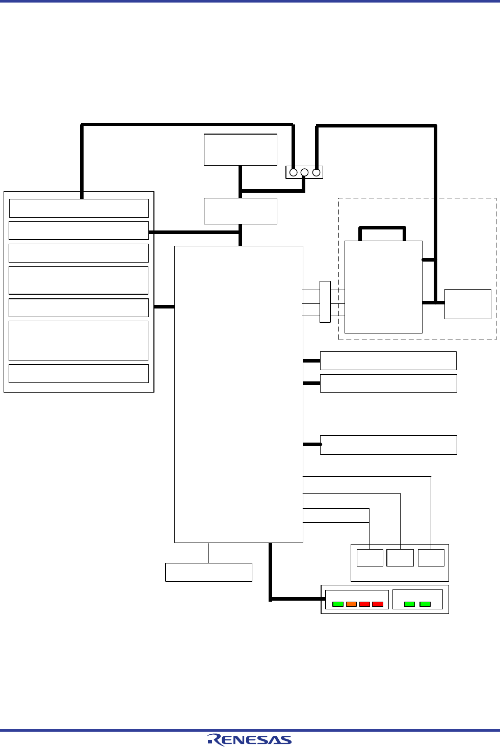
Renesas Solution Starter Kit for RX23W 4. Connectivity
R20UT4446EG0102 Rev. 1.02 Page 15 of 41
Jun 22, 20
4. Connectivity
4.1 Internal Board Connections
The diagram below shows the CPU board components and their connectivity to the MCU.
User Switch (
SW4)
RX23
W
(85
pin)
Microcontroller
IRQ
Reset
ADC I
/O
SW1
SW
2
RES
DC PWR IN
(
5
V)
2Kbit I2
C EEPROM
User LED
Power LED
G
R
O
R
VCC
MCU Mode Switch
(SW
3)
Mode
G
G
Switches
TXD
RXD
USB to Serial
VDD
I
/
O
CTS
/
RTS
Regulator IC
3
.3
V or
1.
8V
FTD
234
XD
VBUS
5
V
Level shift
5V
TXD
RXD
CTS
/
RTS
VCC
Potentiometer
ADTRG*
I
/
O
MCU Header
E1/E2 Lite Debug Interface
CAN
USB
0
(
Host
/
Function
)
Pmod1
(Spare
)*
Pmod
2
(For LCD
)
2.
4GHz RF Antenna
Key x
1
Slider
(Electrode x
4
)
IRQ
3
.3
V
VCCIO
3
V
3
OUT
USB
In addition to DC PWR IN
,
VBUS
(
USB
0
Function
/
USB to Serial
Function) can be used as the power supply source for the board.
* This feature is a not available in the default RS
SK configuration.
Refer to Section 6
for the required modifications.
USB to
Serial
Function
Figure 4-1: Internal Board Block Diagram