
User's Manual
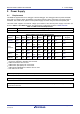
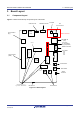
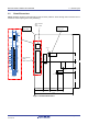
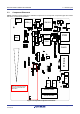
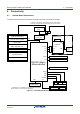
Table Of Contents
- 1. Overview
- 2. Power Supply
- 3. Board Layout
- 4. Connectivity
- 5. User Circuitry
- 6. Configuration
- 6.1 Modifying the RSSK
- 6.2 MCU Operating Modes
- 6.3 E1/E2 Lite Debugger Configuration
- 6.4 Power Supply Configuration
- 6.5 Clock Configuration
- 6.6 Analog Power and ADC Configuration
- 6.7 CAN Configuration
- 6.8 I2C & EEPROM Configuration
- 6.9 IRQ & Switch Configuration
- 6.10 LED Configuration
- 6.11 MCU Header Configuration
- 6.12 PMOD1 Configuration
- 6.13 PMOD2 Configuration
- 6.14 Bluetooth® Low Energy (BLE)
- 6.15 Serial Sound Interface (SSI)
- 6.16 Touch Interface Configuration
- 6.17 USB to Serial Configuration
- 6.18 USB Configuration
- 7. Code Development
- 8. Additional Information
- 9. Certification of Compliance
Renesas Solution Starter Kit for RX23W 3. Board Layout
R20UT4446EG0102 Rev. 1.02 Page 12 of 41
Jun 22, 20
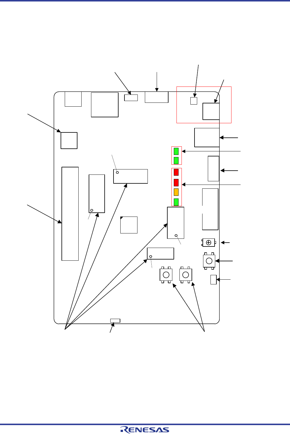
3. Board Layout
3.1 Component Layout
Figure 3-1 below shows the top component layout of the board.
PMOD2
PMOD1
FT234XD
CAN Connector
DC PWR IN
(5V)
User Switches
PMOD1 Connector
Power LEDs
5V_PWR(GREEN)
3V3_PWR(GREEN)
Reset Switch
Potentiometer
USB
Serial
Connector
User LEDs
USB to Serial Port
RX23W
(85pin
BGA)
E1/E2Lite
SW2
SW1
PMOD2 Connector
RF Antenna
VBATT
Connector
Touch Interface
(slider)
USB0
Host
USB0
Function
Touch Interface
(key)
LED3
LED2
LED1
LED0
MCU Header
MCU Header
MCU Header
MCU Header
MCU Header Arrays x 4
e.g.) Grid A2 = RX23W A2 Pin
Grid A2
Grid J1
Grid J3
Grid J9
Figure 3-1: Board Layout