
Users Manual
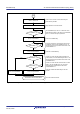
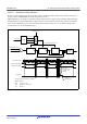
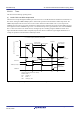
Table Of Contents
- 34. IrDA Interface
- 35. I2C-bus Interface (RIICa)
- 35.1 Overview
- 35.2 Register Descriptions
- 35.2.1 I2C-bus Control Register 1 (ICCR1)
- 35.2.2 I2C-bus Control Register 2 (ICCR2)
- 35.2.3 I2C-bus Mode Register 1 (ICMR1)
- 35.2.4 I2C-bus Mode Register 2 (ICMR2)
- 35.2.5 I2C-bus Mode Register 3 (ICMR3)
- 35.2.6 I2C-bus Function Enable Register (ICFER)
- 35.2.7 I2C-bus Status Enable Register (ICSER)
- 35.2.8 I2C-bus Interrupt Enable Register (ICIER)
- 35.2.9 I2C-bus Status Register 1 (ICSR1)
- 35.2.10 I2C-bus Status Register 2 (ICSR2)
- 35.2.11 Slave Address Register Ly (SARLy) (y = 0 to 2)
- 35.2.12 Slave Address Register Uy (SARUy) (y = 0 to 2)
- 35.2.13 I2C-bus Bit Rate Low-Level Register (ICBRL)
- 35.2.14 I2C-bus Bit Rate High-Level Register (ICBRH)
- 35.2.15 I2C-bus Transmit Data Register (ICDRT)
- 35.2.16 I2C-bus Receive Data Register (ICDRR)
- 35.2.17 I2C-bus Shift Register (ICDRS)
- 35.3 Operation
- 35.4 SCL Synchronization Circuit
- 35.5 SDA Output Delay Function
- 35.6 Digital Noise Filters
- 35.7 Address Match Detection
- 35.8 Automatic Low-Hold Function for SCL
- 35.9 Arbitration-Lost Detection Functions
- 35.10 Start Condition/Restart Condition/Stop Condition Generating Function
- 35.11 Bus Hanging
- 35.12 SMBus Operation
- 35.13 Interrupt Sources
- 35.14 Initialization of Registers and Functions When a Reset is Applied or a Condition is Detected
- 35.15 Event Link Function (Output)
- 35.16 Usage Notes
- 36. CAN Module (RSCAN)

R01UH0823EJ0110 Rev.1.10 Page 1094 of 1852
Nov 30, 2020
RX23W Group 33. Serial Communications Interface (SCIg, SCIh)
33.10.4 Detection of Bus Collisions
Detection of bus collisions operate for cases where output of the Break Field low width and transmission of data are in
progress when the ESMER.ESME bit and the SCI.TE bit are set to 1.
Figure 33.69 shows an example of operations with bus collision detection. Signals output through TXDX12 and input
through RXDX12 are sampled with the bus collision detection clock set with the CR2.BCCS[1:0] bits as the sampling
clock, and the STR.BCDF flag is set to 1 if the signals fail to match three times in a row. An SCIX2 interrupt is also
generated if the value of the ICR.BCDIE bit is 1.
Figure 33.69 Example of Operations with Bus Collision Detection
D
C
QD
C
QD
C
Q
Base clock
Divider
No division
Division by 2
Division by 4
RXDX12 input signal
Bus collision clock
STR.BCDF
CR2.BCCS[1:0]
Bus collision detection clock
Signals not
matching 3 times
confirms a bus
collision.
Write 1 to
STCR.BCDCL
The above diagram assumes the following:
ESMER: ESME = 1
CR2: BCCS[1:0] = 01b
PCR: TXDXPS = 0, RXDXPS = 0
ICR: BCDIE = 1
Match-
detection
circuit
TXDX12 output signal
RXDX12 input signal
TXDX12 output signal