
Users Manual
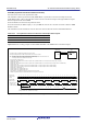
Table Of Contents
- 34. IrDA Interface
- 35. I2C-bus Interface (RIICa)
- 35.1 Overview
- 35.2 Register Descriptions
- 35.2.1 I2C-bus Control Register 1 (ICCR1)
- 35.2.2 I2C-bus Control Register 2 (ICCR2)
- 35.2.3 I2C-bus Mode Register 1 (ICMR1)
- 35.2.4 I2C-bus Mode Register 2 (ICMR2)
- 35.2.5 I2C-bus Mode Register 3 (ICMR3)
- 35.2.6 I2C-bus Function Enable Register (ICFER)
- 35.2.7 I2C-bus Status Enable Register (ICSER)
- 35.2.8 I2C-bus Interrupt Enable Register (ICIER)
- 35.2.9 I2C-bus Status Register 1 (ICSR1)
- 35.2.10 I2C-bus Status Register 2 (ICSR2)
- 35.2.11 Slave Address Register Ly (SARLy) (y = 0 to 2)
- 35.2.12 Slave Address Register Uy (SARUy) (y = 0 to 2)
- 35.2.13 I2C-bus Bit Rate Low-Level Register (ICBRL)
- 35.2.14 I2C-bus Bit Rate High-Level Register (ICBRH)
- 35.2.15 I2C-bus Transmit Data Register (ICDRT)
- 35.2.16 I2C-bus Receive Data Register (ICDRR)
- 35.2.17 I2C-bus Shift Register (ICDRS)
- 35.3 Operation
- 35.4 SCL Synchronization Circuit
- 35.5 SDA Output Delay Function
- 35.6 Digital Noise Filters
- 35.7 Address Match Detection
- 35.8 Automatic Low-Hold Function for SCL
- 35.9 Arbitration-Lost Detection Functions
- 35.10 Start Condition/Restart Condition/Stop Condition Generating Function
- 35.11 Bus Hanging
- 35.12 SMBus Operation
- 35.13 Interrupt Sources
- 35.14 Initialization of Registers and Functions When a Reset is Applied or a Condition is Detected
- 35.15 Event Link Function (Output)
- 35.16 Usage Notes
- 36. CAN Module (RSCAN)

R01UH0823EJ0110 Rev.1.10 Page 1007 of 1852
Nov 30, 2020
RX23W Group 33. Serial Communications Interface (SCIg, SCIh)
BRME Bit (Bit Rate Modulation Enable)
This bit enables and disables the bit rate modulation function. The bit rate generated by on-chip baud rate generator is
evenly corrected when this function is enabled.
NFEN Bit (Digital Noise Filter Function Enable)
This bit enables or disables the digital noise filter function.
When the function is enabled, noise cancellation is applied to the RXDn input signal in asynchronous mode, and noise
cancellation is applied to the SSDAn and SSCLn input signals in simple I
2
C mode.
In any mode other than above, set the NFEN bit to 0 to disable the digital noise filter function.
When the function is disabled, input signals are transferred as is, as internal signals.
BGDM Bit (Baud Rate Generator Double-Speed Mode Select)
Selects the cycle of output clock for the baud rate generator.
This bit is valid when the on-chip baud rate generator is selected as the clock source (SCR.CKE[1] = 0) in asynchronous
mode (SMR.CM = 0). For the clock output from the baud rate generator, either normal or doubled frequency can be
selected. The base clock is generated by the clock output from the baud rate generator. When the BGDM bit is set to 1,
the base clock cycle is halved and the bit rate is doubled.
Set this bit to 0 in modes other than asynchronous mode.
RXDESEL Bit (Asynchronous Start Bit Edge Detection Select)
Selects the detection method of the start bit for reception in asynchronous mode. When a break occurs, data receiving
operation depends on the settings of this bit. Set this bit to 1 when reception should be stopped while a break occurs or
when reception should be started without retaining the RXDn pin input at high level for the period of one data frame or
longer after completion of the break.
Set this bit to 0 in modes other than asynchronous mode.