
Users Manual
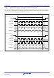
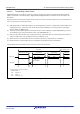
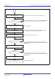
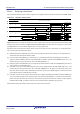
Table Of Contents
- 34. IrDA Interface
- 35. I2C-bus Interface (RIICa)
- 35.1 Overview
- 35.2 Register Descriptions
- 35.2.1 I2C-bus Control Register 1 (ICCR1)
- 35.2.2 I2C-bus Control Register 2 (ICCR2)
- 35.2.3 I2C-bus Mode Register 1 (ICMR1)
- 35.2.4 I2C-bus Mode Register 2 (ICMR2)
- 35.2.5 I2C-bus Mode Register 3 (ICMR3)
- 35.2.6 I2C-bus Function Enable Register (ICFER)
- 35.2.7 I2C-bus Status Enable Register (ICSER)
- 35.2.8 I2C-bus Interrupt Enable Register (ICIER)
- 35.2.9 I2C-bus Status Register 1 (ICSR1)
- 35.2.10 I2C-bus Status Register 2 (ICSR2)
- 35.2.11 Slave Address Register Ly (SARLy) (y = 0 to 2)
- 35.2.12 Slave Address Register Uy (SARUy) (y = 0 to 2)
- 35.2.13 I2C-bus Bit Rate Low-Level Register (ICBRL)
- 35.2.14 I2C-bus Bit Rate High-Level Register (ICBRH)
- 35.2.15 I2C-bus Transmit Data Register (ICDRT)
- 35.2.16 I2C-bus Receive Data Register (ICDRR)
- 35.2.17 I2C-bus Shift Register (ICDRS)
- 35.3 Operation
- 35.4 SCL Synchronization Circuit
- 35.5 SDA Output Delay Function
- 35.6 Digital Noise Filters
- 35.7 Address Match Detection
- 35.8 Automatic Low-Hold Function for SCL
- 35.9 Arbitration-Lost Detection Functions
- 35.10 Start Condition/Restart Condition/Stop Condition Generating Function
- 35.11 Bus Hanging
- 35.12 SMBus Operation
- 35.13 Interrupt Sources
- 35.14 Initialization of Registers and Functions When a Reset is Applied or a Condition is Detected
- 35.15 Event Link Function (Output)
- 35.16 Usage Notes
- 36. CAN Module (RSCAN)

R01UH0823EJ0110 Rev.1.10 Page 1082 of 1852
Nov 30, 2020
RX23W Group 33. Serial Communications Interface (SCIg, SCIh)
33.8.4 Relationship between Clock and Transmit/Receive Data
The CKPOL and CKPH bits in the SPMR register can be used to set up the clock for use in transmission and reception in
four different ways. The relation between the clock signal and the transmission and reception of data is shown in
Figure
33.58
. The relation is the same for both master and slave operation.
Figure 33.58 Relation between Clock Signal and Transmit/Receive Data in Simple SPI Mode
SMISOn pin
SCKn pin
(CKPOL = 1)
Bit 0 Bit 1 Bit 2 Bit 3 Bit 4 Bit 5 Bit 6
Bit 7
SSn# pin
(slave)
SCKn pin
(CKPOL = 0)
(1) When CKPH = 0
SMOSIn pin
SCKn pin
(CKPOL = 1)
Bit 0 Bit 1 Bit 2 Bit 3 Bit 4 Bit 5 Bit 6
Bit 7
SSn# pin
(slave)
SCKn pin
(CKPOL = 0)
(2) When CKPH = 1
SMOSIn pin
Bit 0 Bit 1 Bit 2 Bit 3 Bit 4 Bit 5 Bit 6
Bit 7
Bit 0 Bit 1 Bit 2 Bit 3 Bit 4 Bit 5 Bit 6
Bit 7
SMISOn pin
One unit of transfer data (character or frame)