
Users Manual
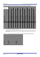
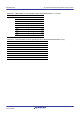
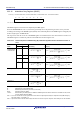
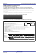
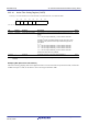
Table Of Contents
- 34. IrDA Interface
- 35. I2C-bus Interface (RIICa)
- 35.1 Overview
- 35.2 Register Descriptions
- 35.2.1 I2C-bus Control Register 1 (ICCR1)
- 35.2.2 I2C-bus Control Register 2 (ICCR2)
- 35.2.3 I2C-bus Mode Register 1 (ICMR1)
- 35.2.4 I2C-bus Mode Register 2 (ICMR2)
- 35.2.5 I2C-bus Mode Register 3 (ICMR3)
- 35.2.6 I2C-bus Function Enable Register (ICFER)
- 35.2.7 I2C-bus Status Enable Register (ICSER)
- 35.2.8 I2C-bus Interrupt Enable Register (ICIER)
- 35.2.9 I2C-bus Status Register 1 (ICSR1)
- 35.2.10 I2C-bus Status Register 2 (ICSR2)
- 35.2.11 Slave Address Register Ly (SARLy) (y = 0 to 2)
- 35.2.12 Slave Address Register Uy (SARUy) (y = 0 to 2)
- 35.2.13 I2C-bus Bit Rate Low-Level Register (ICBRL)
- 35.2.14 I2C-bus Bit Rate High-Level Register (ICBRH)
- 35.2.15 I2C-bus Transmit Data Register (ICDRT)
- 35.2.16 I2C-bus Receive Data Register (ICDRR)
- 35.2.17 I2C-bus Shift Register (ICDRS)
- 35.3 Operation
- 35.4 SCL Synchronization Circuit
- 35.5 SDA Output Delay Function
- 35.6 Digital Noise Filters
- 35.7 Address Match Detection
- 35.8 Automatic Low-Hold Function for SCL
- 35.9 Arbitration-Lost Detection Functions
- 35.10 Start Condition/Restart Condition/Stop Condition Generating Function
- 35.11 Bus Hanging
- 35.12 SMBus Operation
- 35.13 Interrupt Sources
- 35.14 Initialization of Registers and Functions When a Reset is Applied or a Condition is Detected
- 35.15 Event Link Function (Output)
- 35.16 Usage Notes
- 36. CAN Module (RSCAN)

R01UH0823EJ0110 Rev.1.10 Page 1006 of 1852
Nov 30, 2020
RX23W Group 33. Serial Communications Interface (SCIg, SCIh)
ACS0 Bit (Asynchronous Mode Clock Source Select)
Selects the clock source in the asynchronous mode.
The ACS0 bit is valid in asynchronous mode (SMR.CM bit = 0) and when an external clock input is selected
(SCR.CKE[1:0] bits = 10b or 11b). This bit is used to select an external clock input or the logical AND of compare
matches output from the internal TMR.
Set the ACS0 bit to 0 in other than asynchronous mode.
For SCI5 and SCI12, the TMOn output (n = 0, 1) of TMR unit 0 can be set as the base clock source. Refer to
Table
33.25
for details.
The ACS0 bits for SCI1 and SCI8 are reserved. The write values to these bits for SCI1 and SCI8 should be 0.
Figure 33.4 shows a setting example of when TMO0 and TMO1 in the TMR unit 0 are selected for output.
Figure 33.4 Example of Average Transfer Rate Setting When TMR Clock is Input
Table 33.25 Correspondence between SCI Channels and Compare Match Outputs
SCI TMR Compare Match Output
SCI5 Unit 0 TMO0, TMO1
SCI12 Unit 0 TMO0, TMO1
1 bit = Base clock × 16
Average transfer rate = 3 MHz/16 = 187.5 kbps
SCK5 base clock
= 4 MHz × 3/4
= 3 MHz (average)
Clock source
TMO0 output
4 MHz
Clock enable
TMO1 output
Clock source
Clock enable
TMO0
TMO1
TMR (unit 0)
0123 3 3 3 30123012
123 123 123
123 456 789 101112 131415 1612 345
3
4 MHz
3 MHz
012
123
012
123
012
123
012
123
SCI5
SCK5
This figure shows an example when TMR clock is input to SCI5.
When generating 187.5 kbps of TMR average transfer rate for PCLK = 32 MHz:
(1) Generate a frequency of 4 MHz using TMO0 as the clock source.
(2) Set TMO1 in the compare match count of TCNT in TMR0 and generate 3/4 clock enable to set
an average transfer rate of 3 MHz/16 = 187.5 kbps.
Setting examples of TMR and SCI
● TMR0.TCR = 08h (TMR0.TCNT is cleared at compare match in TMR0.TCORA, the count is incremented at rising edge of PCLK/2)
● TMR0.TCCR = 09h
● TMR1.TCR = 08h (TMR1.TCNT is cleared at compare match in TMR1.TCORA, the count is incremented at compare match A in TMR0.TCNT)
● TMR1.TCCR = 18h
● TMR0.TCSR = 09h (0 is output at compare match in TMR0.TCORA, 1 is output at compare match in TMR0.TCORB)
● TMR1.TCSR = 09h (0 is output at compare match in TMR1.TCORA, 1 is output at compare match in TMR1.TCORB)
● TMR0.TCNT = TMR1.TCNT = 0
● TMR0.TCORA = 03h, TMR0.TCORB = 01h
● TMR1.TCORA = 03h, TMR1.TCORB = 00h
● SCR.SCK[1:0] = 10b (External clock input or TMR clock input is selected)
● SEMR = 01h (TMR clock input is selected with 16 base clock cycles for 1-bit period)