
Users Manual
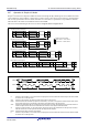
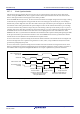
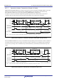
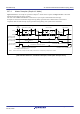
Table Of Contents
- 34. IrDA Interface
- 35. I2C-bus Interface (RIICa)
- 35.1 Overview
- 35.2 Register Descriptions
- 35.2.1 I2C-bus Control Register 1 (ICCR1)
- 35.2.2 I2C-bus Control Register 2 (ICCR2)
- 35.2.3 I2C-bus Mode Register 1 (ICMR1)
- 35.2.4 I2C-bus Mode Register 2 (ICMR2)
- 35.2.5 I2C-bus Mode Register 3 (ICMR3)
- 35.2.6 I2C-bus Function Enable Register (ICFER)
- 35.2.7 I2C-bus Status Enable Register (ICSER)
- 35.2.8 I2C-bus Interrupt Enable Register (ICIER)
- 35.2.9 I2C-bus Status Register 1 (ICSR1)
- 35.2.10 I2C-bus Status Register 2 (ICSR2)
- 35.2.11 Slave Address Register Ly (SARLy) (y = 0 to 2)
- 35.2.12 Slave Address Register Uy (SARUy) (y = 0 to 2)
- 35.2.13 I2C-bus Bit Rate Low-Level Register (ICBRL)
- 35.2.14 I2C-bus Bit Rate High-Level Register (ICBRH)
- 35.2.15 I2C-bus Transmit Data Register (ICDRT)
- 35.2.16 I2C-bus Receive Data Register (ICDRR)
- 35.2.17 I2C-bus Shift Register (ICDRS)
- 35.3 Operation
- 35.4 SCL Synchronization Circuit
- 35.5 SDA Output Delay Function
- 35.6 Digital Noise Filters
- 35.7 Address Match Detection
- 35.8 Automatic Low-Hold Function for SCL
- 35.9 Arbitration-Lost Detection Functions
- 35.10 Start Condition/Restart Condition/Stop Condition Generating Function
- 35.11 Bus Hanging
- 35.12 SMBus Operation
- 35.13 Interrupt Sources
- 35.14 Initialization of Registers and Functions When a Reset is Applied or a Condition is Detected
- 35.15 Event Link Function (Output)
- 35.16 Usage Notes
- 36. CAN Module (RSCAN)

R01UH0823EJ0110 Rev.1.10 Page 1073 of 1852
Nov 30, 2020
RX23W Group 33. Serial Communications Interface (SCIg, SCIh)
33.7.3 SSDA Output Delay
The SIMR1.IICDL[4:0] bits can be used to set a delay for output on the SSDAn pin relative to falling edges of output on
the SSCLn pin. Delay-time settings from 0 to 31 are selectable, representing periods of the corresponding numbers of
cycles of the clock signal from the on-chip baud rate generator (derived by frequency-dividing the base clock, PCLK, by
the divisor selected by the SMR.CKS[1:0] bits). A delay for output on the SSDAn pin is for the start condition/restart
condition/stop condition signal, 8-bit transmit data, and an acknowledge bit.
If the SSDA output delay is shorter than the time for the level on the SSCLn pin to fall, the change of the output on the
SSDAn pin will start while the output level on the SSCLn pin is falling, creating a possibility of erroneous operation for
slave devices. Ensure that settings for the delay of output on the SSDAn pin are for times greater than the time output on
the SSCLn pin takes to fall (300 ns for I
2
C-bus in normal mode and fast mode).
Figure 33.50 shows the timing of delays in SSDA output.
Figure 33.50 Timing of Delays in SSDA Output
Output on the SSCLn pin
Clock signal from the on-chip
baud rate generator (internal signal)
Output on the SSDAn pin
(IICDL[4:0] = 00000b)
Output on the SSDAn pin
(IICDL[4:0] = 00001b)
Output on the SSDAn pin
(IICDL[4:0] = 00010b)
Output on the SSDAn pin
(IICDL[4:0] = 00111b)
Output on the SSDAn pin
(IICDL[4:0] = 01000b)