
Users Manual
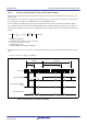
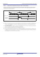
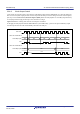
Table Of Contents
- 34. IrDA Interface
- 35. I2C-bus Interface (RIICa)
- 35.1 Overview
- 35.2 Register Descriptions
- 35.2.1 I2C-bus Control Register 1 (ICCR1)
- 35.2.2 I2C-bus Control Register 2 (ICCR2)
- 35.2.3 I2C-bus Mode Register 1 (ICMR1)
- 35.2.4 I2C-bus Mode Register 2 (ICMR2)
- 35.2.5 I2C-bus Mode Register 3 (ICMR3)
- 35.2.6 I2C-bus Function Enable Register (ICFER)
- 35.2.7 I2C-bus Status Enable Register (ICSER)
- 35.2.8 I2C-bus Interrupt Enable Register (ICIER)
- 35.2.9 I2C-bus Status Register 1 (ICSR1)
- 35.2.10 I2C-bus Status Register 2 (ICSR2)
- 35.2.11 Slave Address Register Ly (SARLy) (y = 0 to 2)
- 35.2.12 Slave Address Register Uy (SARUy) (y = 0 to 2)
- 35.2.13 I2C-bus Bit Rate Low-Level Register (ICBRL)
- 35.2.14 I2C-bus Bit Rate High-Level Register (ICBRH)
- 35.2.15 I2C-bus Transmit Data Register (ICDRT)
- 35.2.16 I2C-bus Receive Data Register (ICDRR)
- 35.2.17 I2C-bus Shift Register (ICDRS)
- 35.3 Operation
- 35.4 SCL Synchronization Circuit
- 35.5 SDA Output Delay Function
- 35.6 Digital Noise Filters
- 35.7 Address Match Detection
- 35.8 Automatic Low-Hold Function for SCL
- 35.9 Arbitration-Lost Detection Functions
- 35.10 Start Condition/Restart Condition/Stop Condition Generating Function
- 35.11 Bus Hanging
- 35.12 SMBus Operation
- 35.13 Interrupt Sources
- 35.14 Initialization of Registers and Functions When a Reset is Applied or a Condition is Detected
- 35.15 Event Link Function (Output)
- 35.16 Usage Notes
- 36. CAN Module (RSCAN)

R01UH0823EJ0110 Rev.1.10 Page 1068 of 1852
Nov 30, 2020
RX23W Group 33. Serial Communications Interface (SCIg, SCIh)
33.6.8 Clock Output Control
Clock output can be fixed to high or low using the SCR.CKE[1:0] bits when the SMR.GM bit is 1. When the CKE[1:0]
bits are set to 01b (clock output), the base clock is output from the SCK pin. For the settings of the base clock frequency
(bit rate), refer to
section 33.2.11, Bit Rate Register (BRR). When the CKE[1:0] bits are set to 00b (output fixed low)
or 10b (output fixed to high), the SCK pin can be fixed to low or high.
Figure 33.45 shows a timing chart when the clock output is controlled.
If changing the CKE[1:0] bits while the SMR.GM bit is 0 (non-GSM mode), a pulse of unexpected width may output
from SCK pin because the result is immediately reflected to the SCK pin.
Figure 33.45 Clock Output Control
Base clock
SCR.CKE[1:0] bits
01b 00b 01b
SCR.CKE[1:0] bits 01b 00b 01b 10b 01b
When the SCR.GM bit is 0
When the SCR.GM bit is 1
SCK
SCK
Hi-Z