
Users Manual
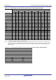
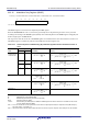
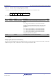
Table Of Contents
- 34. IrDA Interface
- 35. I2C-bus Interface (RIICa)
- 35.1 Overview
- 35.2 Register Descriptions
- 35.2.1 I2C-bus Control Register 1 (ICCR1)
- 35.2.2 I2C-bus Control Register 2 (ICCR2)
- 35.2.3 I2C-bus Mode Register 1 (ICMR1)
- 35.2.4 I2C-bus Mode Register 2 (ICMR2)
- 35.2.5 I2C-bus Mode Register 3 (ICMR3)
- 35.2.6 I2C-bus Function Enable Register (ICFER)
- 35.2.7 I2C-bus Status Enable Register (ICSER)
- 35.2.8 I2C-bus Interrupt Enable Register (ICIER)
- 35.2.9 I2C-bus Status Register 1 (ICSR1)
- 35.2.10 I2C-bus Status Register 2 (ICSR2)
- 35.2.11 Slave Address Register Ly (SARLy) (y = 0 to 2)
- 35.2.12 Slave Address Register Uy (SARUy) (y = 0 to 2)
- 35.2.13 I2C-bus Bit Rate Low-Level Register (ICBRL)
- 35.2.14 I2C-bus Bit Rate High-Level Register (ICBRH)
- 35.2.15 I2C-bus Transmit Data Register (ICDRT)
- 35.2.16 I2C-bus Receive Data Register (ICDRR)
- 35.2.17 I2C-bus Shift Register (ICDRS)
- 35.3 Operation
- 35.4 SCL Synchronization Circuit
- 35.5 SDA Output Delay Function
- 35.6 Digital Noise Filters
- 35.7 Address Match Detection
- 35.8 Automatic Low-Hold Function for SCL
- 35.9 Arbitration-Lost Detection Functions
- 35.10 Start Condition/Restart Condition/Stop Condition Generating Function
- 35.11 Bus Hanging
- 35.12 SMBus Operation
- 35.13 Interrupt Sources
- 35.14 Initialization of Registers and Functions When a Reset is Applied or a Condition is Detected
- 35.15 Event Link Function (Output)
- 35.16 Usage Notes
- 36. CAN Module (RSCAN)

R01UH0823EJ0110 Rev.1.10 Page 1005 of 1852
Nov 30, 2020
RX23W Group 33. Serial Communications Interface (SCIg, SCIh)
Smaller settings of the SMR.CKS[1:0] bits and larger settings of the BRR register reduce difference in the length of the
1-bit period.
33.2.13 Serial Extended Mode Register (SEMR)
Note 1. Writable only when the SCR.TE bit is 0 and the SCR.RE bit is 0 (both serial transmission and reception are disabled).
The SEMR register is used to select a clock source for 1-bit period in asynchronous mode or a detection method of the
start bit.
Address(es): SCI1.SEMR 0008 A027h, SCI5.SEMR 0008 A0A7h, SCI8.SEMR 0008 A107h, SCI12.SEMR 0008 B307h
b7 b6 b5 b4 b3 b2 b1 b0
RXDES
EL
BGDM NFEN ABCS — BRME — ACS0
Value after reset:
00000000
Bit Symbol Bit Name Description R/W
b0 ACS0 Asynchronous Mode
Clock Source Select
(Valid only in asynchronous mode)
0: External clock input
1: Logical AND of two compare matches output from TMR (valid for SCI5
and SCI12 only)
R/W*
1
b1 — Reserved This bit is read as 0. The write value should be 0. R/W
b2 BRME Bit Rate Modulation
Enable
0: Bit rate modulation function is disabled.
1: Bit rate modulation function is enabled.
R/W*
1
b3 — Reserved This bit is read as 0. The write value should be 0. R/W
b4 ABCS Asynchronous Mode
Base Clock Select
(Valid only in asynchronous mode)
0: Selects 16 base clock cycles for 1-bit period.
1: Selects 8 base clock cycles for 1-bit period.
R/W*
1
b5 NFEN Digital Noise Filter
Function Enable
(In asynchronous mode)
0: Noise cancellation function for the RXDn input signal is disabled.
1: Noise cancellation function for the RXDn input signal is enabled.
(in simple I
2
C mode)
0: Noise cancellation function for the SSCLn and SSDAn input signals is
disabled.
1: Noise cancellation function for the SSCLn and SSDAn input signals is
enabled.
The NFEN bit should be 0 in any mode other than above.
R/W*
1
b6 BGDM Baud Rate Generator
Double-Speed Mode
Select
(Only valid the SCR.CKE[1] bit is 0 in asynchronous mode)
0: Baud rate generator outputs the clock with normal frequency.
1: Baud rate generator outputs the clock with doubled frequency.
R/W*
1
b7 RXDESEL Asynchronous Start Bit
Edge Detection Select
(Valid only in asynchronous mode)
0: The low level on the RXDn pin is detected as the start bit.
1: A falling edge on the RXDn pin is detected as the start bit.
R/W*
1